1. STM32 GPIO structure diagram 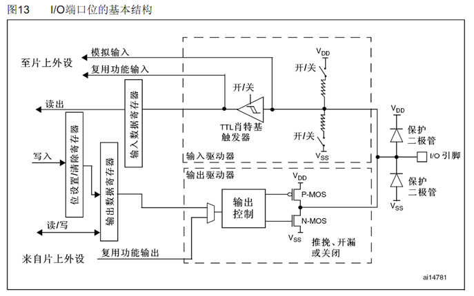
GPIO has 8 setting modes: input floating, input pull-up, input pull-down, analog input, open drain output, push-pull output, push-pull multiplexing function, open drain multiplexing function, a total of 4 inputs, 2 inputs, and 2 multiplexing functions.
2. Mode description
① The Schmitt trigger in the floating input 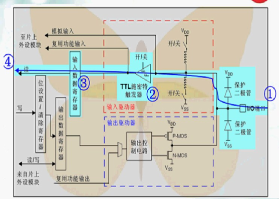
diagram is turned on, the state of the IO port can be directly sent to the input register, and the CPU can directly read the input register;
in the above figure, the shaded part is in a non-working state, especially the output circuit in the lower half, which is actually isolated from the port.
The yellow highlight shows the data transmission channel. The external level signal enters the STM32 through the IO port numbered 1 on the left, and is shaped by the Schmitt trigger numbered 2 and sent to the input data register numbered 3. At the other end of the input data register numbered 4, the CPU can read the level state of the IO port at any time.
② Pull-up input 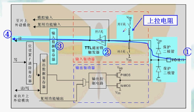
The above figure shows the configuration of the STM32 GPIO with pull-up input mode. Compared with the previous floating input mode, only a pull-up resistor is connected to the upper part of the data channel. According to the STM32 data sheet, the resistance of this pull-up resistor is between 30K and 50K.
Similarly, the CPU can read the level state of the IO port at the other end of the input data register at any time.
③ Pull-down input 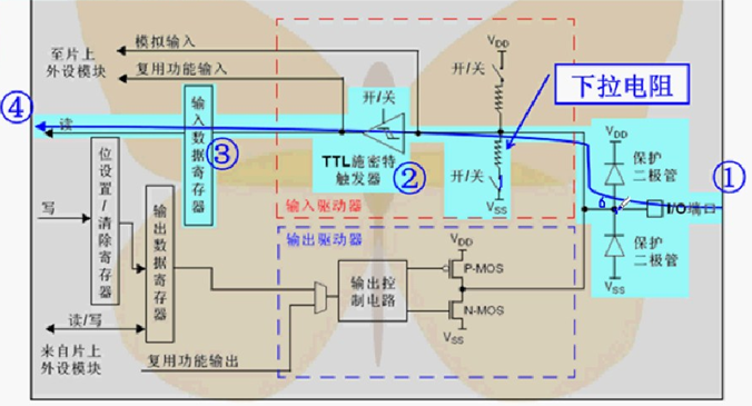
④ The analog input 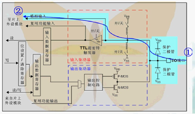
Schmitt trigger is closed, and the signal goes directly to the ADC input;
The configuration of the analog input channel of STM32 is simpler. The signal enters from the port numbered 1 on the left and directly enters the ADC module from the end numbered 2 on the right.
Here we see that all the pull-up, pull-down resistors and Schmitt triggers are in the disconnected state, so the input data register will not reflect the level state on the port, that is, under the analog input configuration, the CPU cannot read valid data on the input data register.
⑤ Open-drain output mode 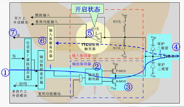
When the CPU writes data at the number 1 end through the "bit set/clear register" or "output data register", the data bit is transmitted to the number 4 IO port through the output control circuit of number 2.
If the CPU writes logic 1, the N-MOS tube No. 3 will be in the off state, and the level of the IO port will be determined by the external pull-up resistor. If the CPU writes logic 0, the N-MOS tube No. 3 will be in the on state, and the level of the IO port will be pulled to the zero potential of VSS by the N-MOS tube No. 3.
In the upper half of the above figure, the Schmitt trigger is in the on state, which means that the CPU can monitor the status of the IO port at any time at the other end of the "input data register"; through this feature, the virtual IO port bidirectional communication is also realized. As long as the CPU outputs logic 1, since the N-MOS tube No. 3 is in the off state, the level of the IO port will be completely determined by the external circuit. Therefore, the CPU can read the signal of the external circuit in the "input data register" instead of the logic 1 output by itself.
In the output mode of the GPIO port, there are 3 output speeds to choose from (2MHz, 10MHz and 50MHz). This speed refers to the response speed of the GPIO port drive circuit, not the speed of the output signal. The speed of the output signal is related to the program (the chip has arranged multiple output drive circuits with different response speeds in the output part of the IO port. Users can choose the appropriate drive circuit according to their needs). By selecting the speed, different output drive modules can be selected to achieve the best noise control and reduce power consumption. High-frequency drive circuits also have high noise. When high output frequency is not required, please use low-frequency drive circuits, which is very helpful to improve the EMI performance of the system. Of course, if you want to output a higher frequency signal, but choose a lower frequency drive module, you may get a distorted output signal.
⑥ Open-drain output multiplexing function 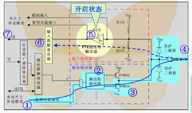
⑦ Push-pull output mode 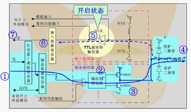
⑧ Push-pull multiplexing output mode 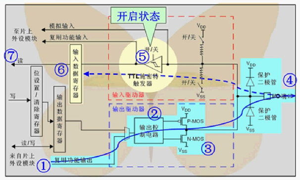
GPIO push-pull multiplexing output mode, the input of the output control circuit No. 2 is connected to the output end of the multiplexing function. At this time, the output data register is disconnected from the output channel and connected to the output signal of the on-chip peripheral. After we configure GPIO to multiplex output function, if the peripheral is not activated, its output will be uncertain, and the other parts are consistent with the above mode, including the reading of "input data register".
3. Application scenarios
① Pull-up input and pull-down input can be used to detect external signals; for example, buttons, etc.;
② Floating input mode, due to the large input impedance, this mode is generally used for the receiving end of I2C and USART of standard communication protocols;
③ Ordinary push-pull output mode is generally used in the occasions where the output level is 0 and 3.3V. The ordinary open-drain output mode is generally used in the occasions where the level does not match. For example, if you need to output a high level of 5V, you need an external pull-up resistor, the power supply is 5V, and the GPIO is set to open-drain mode. When the output is in high impedance state, the pull-up resistor and the power supply output 5V level to the outside.
④ For the corresponding multiplexing mode, it is selected according to the multiplexing function of GPIO. For example, if the GPIO pin is used as the output of the serial port, the multiplexing push-pull output mode is used. If it is used in IC, SMBUS and other occasions where line and function are required, the multiplexing open-drain mode is used.
⑤When using any open-drain mode, a pull-up resistor is required.
Previous article:STM32 GPIO port input mode configuration example
Next article:Problems with setting pull-up and pull-down in GPIO_PuPd register in STM32F4
Recommended ReadingLatest update time:2024-11-16 20:57

![[STM32 motor square wave] Record 3——TIM1 time base initialization configuration](https://6.eewimg.cn/news/statics/images/loading.gif)
- Popular Resources
- Popular amplifiers
 Professor at Beihang University, dedicated to promoting microcontrollers and embedded systems for over 20 years.
- Innolux's intelligent steer-by-wire solution makes cars smarter and safer
- 8051 MCU - Parity Check
- How to efficiently balance the sensitivity of tactile sensing interfaces
- What should I do if the servo motor shakes? What causes the servo motor to shake quickly?
- 【Brushless Motor】Analysis of three-phase BLDC motor and sharing of two popular development boards
- Midea Industrial Technology's subsidiaries Clou Electronics and Hekang New Energy jointly appeared at the Munich Battery Energy Storage Exhibition and Solar Energy Exhibition
- Guoxin Sichen | Application of ferroelectric memory PB85RS2MC in power battery management, with a capacity of 2M
- Analysis of common faults of frequency converter
- In a head-on competition with Qualcomm, what kind of cockpit products has Intel come up with?
- Dalian Rongke's all-vanadium liquid flow battery energy storage equipment industrialization project has entered the sprint stage before production
- Allegro MicroSystems Introduces Advanced Magnetic and Inductive Position Sensing Solutions at Electronica 2024
- Car key in the left hand, liveness detection radar in the right hand, UWB is imperative for cars!
- After a decade of rapid development, domestic CIS has entered the market
- Aegis Dagger Battery + Thor EM-i Super Hybrid, Geely New Energy has thrown out two "king bombs"
- A brief discussion on functional safety - fault, error, and failure
- In the smart car 2.0 cycle, these core industry chains are facing major opportunities!
- The United States and Japan are developing new batteries. CATL faces challenges? How should China's new energy battery industry respond?
- Murata launches high-precision 6-axis inertial sensor for automobiles
- Ford patents pre-charge alarm to help save costs and respond to emergencies
- New real-time microcontroller system from Texas Instruments enables smarter processing in automotive and industrial applications
- EEWORLD University ---- designing electrical systems vol 1
- Rice goes in and rice comes out. How is rice husked? You may not have seen it even if you have been eating it for decades!
- The gap between actual power supply and ideal power supply
- Is it possible for the LDO or DCDC output voltage to be lower than the internal reference voltage?
- Okay, let’s talk about the Internet of Things technology protocol
- On-line debugging method for embedded processors
- PCB issues for switching power supplies
- [Zero-knowledge ESP8266 tutorial] Quick start 21 world clock demo
- A question about the schematic
- National College Student Electronic Design Competition Open Source Flight Control Data Album: APM Learning Materials

 usb_host_device_code
 Transplantation of real-time operating system RT-ThreadSmart on STM32MP1


 京公网安备 11010802033920号