1 Introduction:
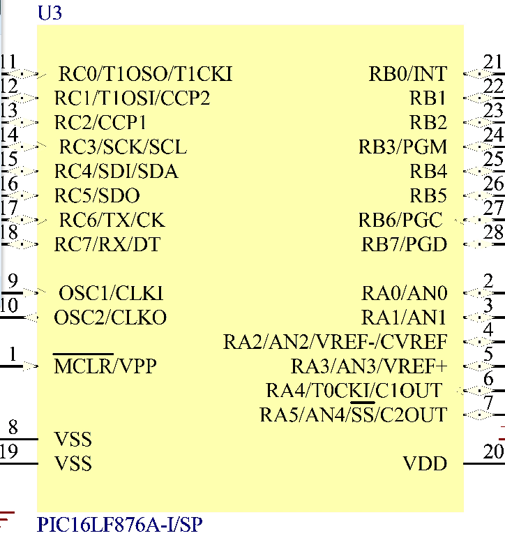
PIC microcontroller pin diagram:
In the PIC16F87X microcontroller, the 28-pin microcontroller has 3 I/O ports, namely RA, RB and RC; the 40-pin microcontroller has 5 I/O ports, namely RA, RB, RC, RD and RE. Among them, RA has 6 lines, RE has 3 lines, and the rest have 8 lines. The port
lines of the PIC16F87X port can be used as ordinary I/O pins, and can also be used as external pins of certain components or peripheral modules. For example, port pin RC.4 can be used as an ordinary I/O pin, and can also be used as a data input pin for SPI serial communication. Here we only introduce the basic functions and basic usage of the port, and other complex functions of the port will be introduced later.
2. Two registers related to input/output ports
Each I/O port in the PIC microcontroller has two basic dedicated registers: port data register and port direction register, as shown below.
These registers have a unified address in RAM, that is, the ports of the PIC microcontroller can be accessed as RAM units without the need for special instructions.
3. Basic structure of input/output ports
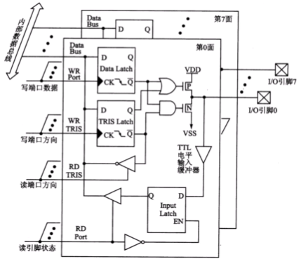
The 3/5 ports of PIC16F87X not only have structural differences, but the internal structures of the lines of the same port are also slightly different. However, their basic structural model is shown in the figure below.
There are three D flip-flops (also called latches) in the diagram.
Where Data Latch represents the port data register, such as PORTA, PORTB, PORTC;
TRIS Latch port direction register, such as TRISA, TRISB, TRISC; and Input Latch is used as a buffer when the port is set to input.
3.1 Working Principle of Basic Input/Output Ports
The following are the basic operations on the port line:
⒈Write the I/O direction register TRIS Latch.
When the content in the direction register is 1, the corresponding port line is set to input (Input); when its content is 0, the corresponding pin is set to output (Output).
⒉ To output data through the port pin
, the port line must be set as output in advance, that is, the content of the corresponding TRIS Latch must be 0.
⒊
To input data from the port pin, the port line must be set as input in advance, that is, the content of the corresponding TRIS Latch must be 1.3.2 Application examples of basic functions of input/output ports
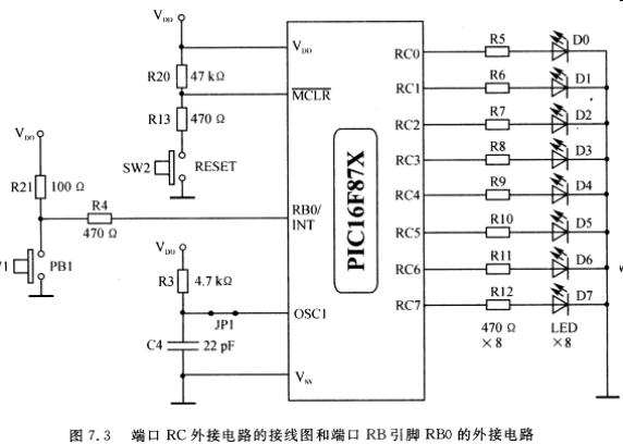
The following example is a single-touch-triggered 8-bit binary cumulative counter, which is designed based on the port function and the hardware on the ICD online debugger. The hardware circuit used in this example is shown in the figure below.
In the figure, port RC is connected to 8 branches, which constitute the output circuit of port RC. Among them, 8 resistors play a current limiting role to protect the port pins and the light-emitting diode LED; the LED emits light at a high level. The figure also uses the RB0 line of port RB as an external input pin. Resistor R4 is a current limiting resistor, which protects the RB0 pin; resistor R21 is a pull-up resistor, which pulls the RB0 level up; switch SW1 is used to manually input a low-level pulse signal.
Programming ideas:
When the power is just turned on, all 8 LEDs are off, indicating that the initial value of the counter is 0.
When the switch SW1 is pressed, the counter value increases by 1, D0 lights up, indicating the binary number 00000001B, and then the button is released; when SW1 is pressed again, the counter value increases by 1, D1 lights up, indicating the binary number 00000010B, and then the button is released again; and so on. When the button is pressed 255 times, D7~D0 all light up, and if the button is pressed again, the counter will return to 0. This cycle repeats.When designing a button input program, one thing you need to pay attention to is that you must handle the jitter phenomenon when the button is pressed or released to avoid misjudgment. The de-jitter of a button is generally eliminated by calling a delay program. That is, in the program design, when the first level change on RB0 is queried, it is immediately delayed by τ (for example, 10ms), and after the state on RB0 is stable, it is queried again to confirm that it is a key action (pressed or released), it is considered valid, otherwise, it is judged as an interference pulse. The program list is as follows:
STATUS EQU 03H
PORTB EQU 06H
TRISB EQU 86H
PORTC EQU 07H
TRISC EQU 87H
DATA1 EQU 20H; DATA1 is a delay variable
DATA2 EQU 21H; DATA2 is a delay variable
N1 EQU D'13' ;Outer loop delay constant
N2 EQU 0FFH ; Inner loop delay constant
RP0 EQU 5H; Body selection position RP0
ORG 000H
BSF STATUS, RP0 ; switch to RAM bank 1
MOVLW 00H ; Set port C as output
MOVWF TRISC
MOVLW 0FFH ; Set port B as input
MOVWF TRISB
BCF STATUS, RP0 ; Restore to RAM volume 0
Assembly language often requires more hardware knowledge, so for people who focus on software or have good C language programming skills, I prefer C programming.
The following is a program written in C language:
include
#define N1 13 //External loop
#define N2 0xff //Inner loop
static volatile bit PORTB0 @(unsigned)&PORTB*8+0; //Port variable design
int DATA1,DATA2;
main() {
TRISC=0xff; //Input ??????? TRISC = 0x00; //Output
TRISB=0xff; //Input
PORTC=0; //Clear
check: if PORTB0==0 then goto check; //Monitor whether there is a level signal input Valid level signal 1
DELAY(); //Delay de-jitter
if PORTB0==0 then goto check; //debounce confirmation
PORTC++; //The advantages of C language design are immediately apparent
CHECK1 if PORTB0==1 goto CHECK1;
DELAY()
if PORTB0==1 goto CHECK1;
GOTO check;
while(1) { };
}
void DELAY()
{
DATA1=N1;
LP0: DATA2=N2;
LP1: if DATA2-- > 0 goto LP1;
if DATA1-- > 0 goto LP0;
return;
}
Previous article:PIC Microcontroller Introduction_8-bit AD Converter
Next article:PIC microcontroller introduction_PICC pointer to RAM
- Popular Resources
- Popular amplifiers
- Naxin Micro and Xinxian jointly launched the NS800RT series of real-time control MCUs
- How to learn embedded systems based on ARM platform
- Summary of jffs2_scan_eraseblock issues
- Application of SPCOMM Control in Serial Communication of Delphi7.0
- Using TComm component to realize serial communication in Delphi environment
- Bar chart code for embedded development practices
- Embedded Development Learning (10)
- Embedded Development Learning (8)
- Embedded Development Learning (6)
 Professor at Beihang University, dedicated to promoting microcontrollers and embedded systems for over 20 years.
- Intel promotes AI with multi-dimensional efforts in technology, application, and ecology
- ChinaJoy Qualcomm Snapdragon Theme Pavilion takes you to experience the new changes in digital entertainment in the 5G era
- Infineon's latest generation IGBT technology platform enables precise control of speed and position
- Two test methods for LED lighting life
- Don't Let Lightning Induced Surges Scare You
- Application of brushless motor controller ML4425/4426
- Easy identification of LED power supply quality
- World's first integrated photovoltaic solar system completed in Israel
- Sliding window mean filter for avr microcontroller AD conversion
- What does call mean in the detailed explanation of ABB robot programming instructions?
- STMicroelectronics discloses its 2027-2028 financial model and path to achieve its 2030 goals
- 2024 China Automotive Charging and Battery Swapping Ecosystem Conference held in Taiyuan
- State-owned enterprises team up to invest in solid-state battery giant
- The evolution of electronic and electrical architecture is accelerating
- The first! National Automotive Chip Quality Inspection Center established
- BYD releases self-developed automotive chip using 4nm process, with a running score of up to 1.15 million
- GEODNET launches GEO-PULSE, a car GPS navigation device
- Should Chinese car companies develop their own high-computing chips?
- Infineon and Siemens combine embedded automotive software platform with microcontrollers to provide the necessary functions for next-generation SDVs
- Continental launches invisible biometric sensor display to monitor passengers' vital signs
- Live Review: TI Ultrasonic Gas Flow Measurement Innovation Solution + CC13X2/CC26X2
- YX009K-8D switch RGB colorful control example
- What a mess it is to have a 0.1uf capacitor with a problem {Complain about this here}
- How can the Gibbs effect be mitigated?
- Wuhan plague, the possibility of third, fourth, fifth and sixth generation infection cases
- [RISC-V MCU CH32V103 Evaluation] Design of Light Intensity Recorder (and Final Report)
- Fudan Micro FM33LC046N Review + RTC Clock
- PCB impedance control experience sharing
- Domestic sewage treatment online monitoring system
- Write down your 2021 plan, put it into practice together, and become a better you and me!


 singlechip-implementation-of-levelcrossing-adc-for-ecg-sampling-2332-0796-1000219


 京公网安备 11010802033920号