STM8S is a microcontroller based on an 8-bit framework structure. Its CPU core has 6 internal registers, through which data can be processed efficiently. The STM8S instruction set supports 80 basic 20 addressing modes, and the 6 internal registers of the CPU have addressable addresses. If you want to know the entire STM8S instruction set, please refer to the STM8 Microcontroller Family Programming Manual (PM0044). CPU Registers
Six CPU registers can be seen in the programming model shown in Figure 1. After an interrupt occurs, the registers are pushed onto the stack in the order shown in Figure 2, and they are popped off the stack in the reverse order. If necessary, the interrupt service routine can use POP and PUSH instructions to operate on them.
CPU Register Description
Accumulator (A)
The accumulator is an 8-bit general-purpose register used to store operands and results of arithmetic, logical and data operations.
Index registers (X and Y)
X and Y are both 16-bit registers that enable efficient addressing modes. They can also be used as temporary registers for data operations and for operations such as multiplication and division. In most cases, the cross assembler generates a PRECODE instruction in the instruction code that uses the Y register to distinguish it from the instruction that uses the X register.
Program counter (PC)
The program counter is a 24-bit register that stores the address of the next instruction to be executed by the CPU. Its contents are automatically refreshed after each instruction operation. Since the program pointer has 24 bits, the maximum addressing range of STM8 can reach 16M bytes.

figure 1)
Stack Pointer (SP)
The stack pointer is a 16-bit register whose content is the address of the next freely allocable location in the stack. Depending on the model, the upper bits of the stack pointer have a specific preset value.
The stack is generally used to store the CPU context (program counter, key registers, parameters of related functions and local variables, etc.) during interrupt calls or subroutine calls. The user can also directly operate on the stack through POP and PUSH instructions.
The SP can be initialized by the startup code of the C compiler, and the C language application will initialize it according to the link file containing absolute address information used by the user. If the user uses a link file and startup code written by the user, please make sure that the SP is initialized properly (please refer to the corresponding data sheet for specific address information). After the MCU is reset or after the stack reset instruction (RSP) is executed, the stack pointer is set to its maximum allowed value. For applications using assembly language, the user can use the startup code provided by ST or write his own startup code to initialize the SP correctly.
Push operations decrement the stack pointer value, and pop operations increase the stack pointer value. When the stack pointer value is at its minimum allowed value, further stacking will cause the stack pointer value to wrap around to its maximum value, which will cause previously stored data to be overwritten, but there is no interrupt or hardware flag to indicate this event. The application needs to ensure that the stack is operated correctly and there is no overflow.
Subroutine calls take up 2 or 3 bytes of space. Interrupt calls take up 9 bytes of space to store internal registers (except SP). Please refer to Figure 2.

figure 2)
*Note: The WFI/HLAT instruction will save the CPU context in advance. If an interrupt occurs while the CPU is in WFI or HALT state, the latency required to enter the interrupt will be reduced accordingly.
- Condition Code Register (CC)
The condition code register is an 8-bit register used to indicate the result of the instruction just executed and the status of the processor. The 7th bit (MSB) of the register is a reserved bit. These bits can be tested individually by the user's program or code, and the test results can be used to indicate the status after the program or code is executed. The following paragraphs will describe the meaning of each bit.- V: Overflow
In the last signed arithmetic operation, if an overflow occurs in the highest bit of the result, this bit is set to 1. Please refer to INC, INCW, DEC, DECW, NEG, NEGW, ADD, ADDW, ADC, SUB, SUBW, SBC, CP, CPW and other instructions.

Table 1)
I1: Interrupt mask level 1
I1 and I0 are used together to indicate the interruptibility of the CPU in the current state, please refer to Table 1. I1 and I0 can be set or cleared by executing RIM, SIM, HALT, WFI, IRET, TRAP and POP instructions. I1 and I0 will also be automatically set to the interrupt level corresponding to the interrupt by the hardware when the CPU enters the interrupt service routine. - V: Overflow
- H: Half Carry
During the ADD or ADC operation, when a carry occurs between the 3rd and 4th bits of the ALU, the H bit is set to 1, which is
very meaningful for BCD code arithmetic operations. - I0: Interrupt mask level 0,
please refer to Table 1. - N: Negative number
When the result of the last arithmetic, logical, or data operation is negative, the N bit is set to 1 (for example, the highest bit of the result is logical 1). - Z: Zero
When the result of the last arithmetic, logical, or data operation is zero, the Z bit is set to 1. - C: Carry
This bit is set to 1 if a carry or borrow occurs in the highest bit of the result in the last arithmetic operation. This bit is also affected when executing bit test, branch, shift, rotate, and load instructions. Please refer to instructions such as ADD, ADC, SUB, SBC, etc.
In division operations, the C bit is used to indicate whether an error occurred during instruction execution (quotient overflow or divisor 0). Please refer to the DIV instruction.
In bit test operations, the tested bit is copied to the C bit; please refer to the BTJF, BTJT instructions. In shift and rotate operations, the C bit is updated accordingly based on the result; please refer to the RRC, RLC, SRL, SLL, SRA instructions.
Users can also set, clear, and invert the C bit through the SCF, RCF, CCF instructions.
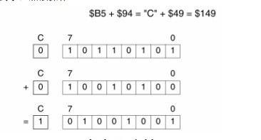
Example: Addition operation
Previous article:STM8 storage FLASH, EEPROM, storage protection
Next article:MCU expert decrypts: Where is the instruction data written?
- Popular Resources
- Popular amplifiers
- Learn ARM development(16)
- Learn ARM development(17)
- Learn ARM development(18)
- Embedded system debugging simulation tool
- A small question that has been bothering me recently has finally been solved~~
- Learn ARM development (1)
- Learn ARM development (2)
- Learn ARM development (4)
- Learn ARM development (6)
 Professor at Beihang University, dedicated to promoting microcontrollers and embedded systems for over 20 years.
- LED chemical incompatibility test to see which chemicals LEDs can be used with
- Application of ARM9 hardware coprocessor on WinCE embedded motherboard
- What are the key points for selecting rotor flowmeter?
- LM317 high power charger circuit
- A brief analysis of Embest's application and development of embedded medical devices
- Single-phase RC protection circuit
- stm32 PVD programmable voltage monitor
- Introduction and measurement of edge trigger and level trigger of 51 single chip microcomputer
- Improved design of Linux system software shell protection technology
- What to do if the ABB robot protection device stops
- Why software-defined vehicles transform cars from tools into living spaces
- How Lucid is overtaking Tesla with smaller motors
- Wi-Fi 8 specification is on the way: 2.4/5/6GHz triple-band operation
- Wi-Fi 8 specification is on the way: 2.4/5/6GHz triple-band operation
- Vietnam's chip packaging and testing business is growing, and supply-side fragmentation is splitting the market
- Vietnam's chip packaging and testing business is growing, and supply-side fragmentation is splitting the market
- Three steps to govern hybrid multicloud environments
- Three steps to govern hybrid multicloud environments
- Microchip Accelerates Real-Time Edge AI Deployment with NVIDIA Holoscan Platform
- Microchip Accelerates Real-Time Edge AI Deployment with NVIDIA Holoscan Platform
- EEWORLD University Hall----Live Replay: TI Wireless Product Update: Wi-Sun Standard Helps Smart City Construction
- TI automotive solution puzzle, do you dare to challenge it?
- [Fifth Batch of Shortlist] GigaDevice GD32L233 Review Event
- [SAMR21 new gameplay] 8. Serial communication-1
- Mobile station update development board, welcome to borrow it!!
- 3. "Wanli" Raspberry Pi car - Python learning (timing task)
- This is a camera development board, but where is the camera?
- Sharing the principle of the adapter solution for charging while listening to music
- Make announces its return
- The mysterious EMC, how did it come about?


 OP215AZ/883C


 京公网安备 11010802033920号