0 Introduction
Special integrated switching power supplies mainly include the following five types [1]:
1) Composite switching power supply;
2) Constant voltage/constant current (CV/CC) switching power supply;
3) Cut-off output type switching power supply;
4) Constant power output switching power supply;
5) Other special switching power supplies, such as high-speed modem power supply, DVD power supply, etc.
There are two design options for special monolithic switching power supplies: the first is to use a general-purpose monolithic switching power supply integrated circuit (such as TOPSwitch-II, TOPSwitch-FX, TOPSwitch-GX series), and then add peripheral circuits such as a voltage control loop and a current control loop. Its characteristics are high output power but complex peripheral circuits. The second is to use the recently launched LinkSwitch series of high-efficiency constant voltage/constant current three-terminal monolithic switching power supply chips, or to use LinkSwitch-TN series, DPA-Switch series monolithic switching power supply dedicated ICs [2]. This can greatly simplify the circuit and reduce costs, making it suitable for the construction of medium and small power special switching power supplies.
1 2.5W constant voltage/constant current charger module
The following is a 2.5W constant voltage/constant current charger module composed of LNK500. It is suitable for mobile phone battery chargers, personal digital assistants (PDA, Personal Digital Assistant), portable audio equipment, electric shavers, built-in power supplies of household appliances (such as backup power and bias power supplies of color TVs) and other fields.
1.1 Performance characteristics and technical indicators
1) Using high-efficiency constant voltage/constant current monolithic switching power supply LNK500, the AC input voltage range is 85~265V. When the AC input voltage is 265V, the leakage current is <5μA, the rated output voltage is 5.5V, the maximum output current is 0.45A, and the output power is 2.5W.
2) Low power consumption, high efficiency, no-load power consumption <0.3W, the typical value of power efficiency η≈68%.
3) At the peak power point, the output voltage is allowed to have an error of ±10%. When the error of the primary inductance Lp is ±10%, the output current has an error of ±25%.
4) The circuit is simple and inexpensive. The power supply only requires 23 components and does not require a secondary feedback circuit. Constant current/constant voltage output can be achieved using the primary circuit, allowing the use of a low-cost, small-size EE13 type magnetic core.
5) With overheat protection, output short circuit protection and open loop protection functions.
6) Comply with the international electromagnetic compatibility standard CISPR22B/EN55022B.
1.2 Circuit Design of 2.5W Constant Voltage/Constant Current Charger Module
The internal circuit of the 2.5W constant voltage/constant current charger module composed of LNK500 is shown in Figure 1. FR is a self-recoverable fuse resistor, which has a current limiting protection function and can limit the impact current when power is on. VD1~VD4 constitute a bridge rectifier, and the inductor L1, L2 and the capacitor C1, C2 form a low-power π-type filter, which can filter out electromagnetic interference. L2 can use a 3.3μH magnetic bead. When the power MOSFET inside LNK500 is turned on, the output rectifier tube VD6 is turned off, and the electric energy is stored in the high-frequency transformer. When the power MOSFET is turned off, VD6 is turned on, and the energy stored in the high-frequency transformer is output through the secondary circuit. VD6 uses a 1A/100V Schottky diode SB1100. R4 and C7 are connected in parallel at both ends of VD6 to prevent VD6 from self-excited oscillation in the high-frequency switching state. C6 is the output filter capacitor. R5 is a 22kΩ load resistor.
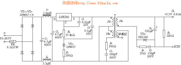
Figure 1 Internal circuit of a 2.5W constant voltage/constant current charger module
The RCD clamp circuit composed of R1, C3 and VD5 has the following functions:
1) When the power MOSFET is turned off, the primary inductive voltage is clamped;
2) It can simplify the design of the feedback circuit.
The feedback current of the control terminal is set by resistor R2. When the power is just started, the control terminal capacitor C4 supplies power to LNK500, and C4 also determines the automatic restart frequency.
In order to reduce electromagnetic interference, the primary of the high-frequency transformer is designed with two windings, NP1 and NP2. NP2 is called the "cancellation winding", which is connected to the primary return end through R3 and C5 to reduce electromagnetic interference in the primary circuit. In addition, a shielding layer needs to be added between the primary and secondary.
LNK500 is only suitable for working in discontinuous mode, and its output power is determined by formula (1).
PO≈0.5ηLPIP2f(1)
Where: PO is the output power;
η is the power efficiency;
LP is the primary inductance of the high-frequency transformer;
IP is the peak current of LNK500;
f is the switching frequency.
It is not difficult to see that PO is proportional to LP, and the size of IP2f is controlled by LNK500.
The high-frequency transformer uses EE13 type magnetic core with 8-pin skeleton. The primary winding NP1 is wound with 90 turns of φ0.13mm enameled wire, NP2 is wound with 22 turns of φ0.16mm enameled wire, and the secondary winding is wound with 5 turns of two strands of φ0.25mm triple insulated wire. Three strands of φ0.25mm enameled wire are wound with 5 turns between the primary and secondary windings as a shielding layer. The primary inductance LP=2.3mH (±10% error is allowed). The resonant frequency of the high-frequency transformer is not less than 300kHz. [page]
The output characteristics of a 2.5W constant voltage/constant current charger are shown in Figure 2.
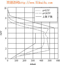
Figure 2 Constant voltage/constant current output characteristics of a 2.5W charger
2 15W DC/DC power converter module with Ethernet interface
2.1 Performance characteristics of Ethernet power
Ethernet (EthernetNetwork) is the most commonly used local area network. Ethernet power is referred to as POE (Power Over Ethernet). It can provide users with data and power supply at the same time through only one Ethernet cable, without the need for additional wiring. The power supply device in the Ethernet power supply is referred to as PD, which has the following characteristics:
——Can provide PD detection and classification signals;
——Can provide soft start interface to DC/DC power converter;
——It has functions such as over-current protection, over-voltage protection and over-heat protection.
According to the POE specification, PD should have the following 3 basic functions.
1) Ability to identify signal impedance When an input voltage is applied to the PD, it must present the correct identification signal impedance within the specified voltage range. When an Ethernet device requests power, it first sends a 2.5-10V voltage signal to the Ethernet. After the effective PD detects this voltage signal, it places a 23.75-26.25kΩ resistor in the power supply loop, and the current will change with the input voltage; by detecting this current, it is confirmed that there is a valid Ethernet device that needs power at the Ethernet cable terminal. If the placed resistor value is in the range of 12-23.75kΩ or 26.25-45kΩ, the Ethernet device is considered valid but does not need power. Resistance values in other ranges mean that the detected Ethernet device is invalid.
2) Type There are different types of PDs, each type corresponds to a certain current. For example, the current of a "0" type PD is 0.5-4mA. After the PD detects a valid signal, it is classified. The specific method is to increase the voltage sent to the network link to 15.5-20.5V so that the PD obtains a fixed current, and then complete the PD classification based on the current range.
3) Switch connection There are two main types of switches for connecting Ethernet power. One is a bipolar transistor switch, which has high power efficiency and low cost; the other is a MOSFET switch, which has extremely high power efficiency (close to 100%).
The following introduces a synchronous rectification 15W DC/DC power converter module with Ethernet interface circuit, which can be widely used in network and communication equipment.
2.2 Circuit Design of 15W Ethernet Power Module
The internal circuit of the 15WPOE module composed of a bipolar switch tube and DPA424P is shown in Figure 3. The power supply consists of two parts, namely the Ethernet interface circuit (represented by a dotted box in the circuit) and the DC/DC power converter. The module contains the POE identification signal impedance (24.9kΩ, DC 2.5~10V) and the "Class 0" type circuit (0.5~4mA, DC 15~20V). When using a bipolar transistor switch or a MOSFET switch, the efficiency of the POE interface is η≥87% or η≥97% respectively.
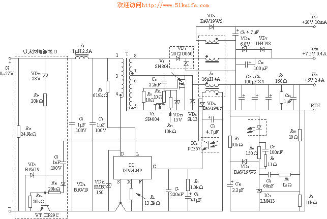
Figure 3: Internal circuit of 15WPOE module composed of bipolar switch tube and DPA424P
2.2.1 Working Principle of Ethernet Power Interface Circuit
The working process of the Ethernet power interface circuit can be divided into three stages: In the first stage, when the input voltage is applied to the PD, it must present the correct identification signal impedance within the voltage range of 2.5 to 10V DC, and the resistor R13 (24.9kΩ) can provide this impedance; In the second stage, when the DC input voltage is 15 to 20V, the PD uses a specified current to identify the device type, for example, the "Class 0" current range is 0.5mA to 4mA, which is also completed by R13; In the third stage, the input voltage is connected to the DC/DC power converter through the bipolar switch tube (VT), and the power converter allows the input of a DC voltage exceeding 30V (28V + UR14). At this time, the voltage regulator tube VDZ1 is reversely broken down, and the base current is provided to VT through R14. The function of R15 is to prevent the power supply from being turned on under other conditions. Once the power supply is turned on, the high-frequency voltage signal output by the auxiliary winding passes through the coupling capacitor C3, the rectifier tube VD2 and the current limiting resistor R16 to increase the DC bias of VT and increase the base current. VD1 is turned on during the negative half cycle, ensuring that the bias voltage applied to the base is always positive.
As shown in Figure 4, a switch circuit using MOSFET (V3) is shown. VDZ4 and VDZ5 use 28V and 15V voltage regulators respectively. When the input voltage exceeds 28V, VDZ4 is reversely broken down, causing V3 to conduct and turn on the power supply. When the input voltage exceeds 43V, VDZ5 is also reversely broken down, which can limit the gate-source voltage of V3 and play a protective role. R15 can prevent V3 from being mis-turned on. The relationship curve between the identification signal impedance and the input voltage of the Ethernet power module is shown in Figure 5, and the identification voltage range is 2.5~10V.
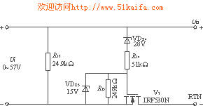
Figure 4 Switching circuit using MOSFET
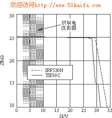
Figure 5 Relationship curve between identification signal impedance and input voltage [page]
2.2.2 Working Principle of 15WDC/DC Power Converter
The main performance indicators of DC/DC power converter are as follows:
1) Use DPA424P type monolithic switching regulator to form a forward, isolated, 3-way output DC/DC power converter module. The DC input voltage range is 36~75V, the 3-way output is 5V/2.4A, 7.5V/0.4A and 20V/10mA respectively, the total output power is 15.2W, and the switching frequency is 400kHz;
2) Multiple outputs, good voltage regulation performance. In the worst case, the load regulation rate indicators of each output are shown in Table 1.
Table 1 Load regulation index of each output
| 3 output voltages UO/V | 5 | 7.5 | 20 |
|---|---|---|---|
| Load variation range/% | 20~100 | 0~100 | 100 |
| Load regulation SI/% | ≤±1 | -4~+8 | -3~+6 |
4) Can accurately set the undervoltage and overvoltage values of the input line;
5) It has output overload protection, open loop protection and overheat protection functions.
In Figure 3, the input EMI filter is composed of C1, L1 and C2. R1 is the undervoltage/overvoltage setting resistor, and the set UUV=33.3V, UOV=86.0V. R1 can also automatically reduce the maximum duty cycle to prevent magnetic saturation. R2 is the limit current setting resistor. When R2=13.3kΩ, the set drain limit current ILIMIT′=0.57ILIMIT=0.57×2.50A=1.425A. The voltage regulator VDZ2 can clamp the drain voltage within a safe range. The equivalent gate capacitance of V1 can provide the best reset for the high-frequency transformer.
The power supply uses 5V output as the main output, and the other two outputs are obtained on this basis. C11, R11, R12 and MOS field effect tubes V2 and V1 form a capacitor-coupled synchronous rectifier for the 5V main output. The voltage regulator VDZ3 plays a clamping role. When there is no switching signal, V2 is turned off through the pull-down resistor R13. The voltage of the flyback winding of the energy storage inductor L2 is rectified and filtered by VD4 and C9 to obtain a 20V output. The voltage of the secondary winding (8-5) of the high-frequency transformer is rectified and filtered by VD3 and C10 to obtain a 7.5V output. The 6.8V voltage regulator VDZ4 and the diode VD7 are connected in series with reverse polarity as the load resistor of the 7.5V output to improve the no-load voltage regulation characteristics. Once the output voltage exceeds 7.5V at no-load, VDZ4 is reversely broken down, and the output voltage can be clamped to about 7.5V by using the voltage drop across VDZ4 and VD2. In normal operation, the output voltage of the auxiliary winding is rectified and filtered by VD6 and C5 to provide a 12-15V bias voltage to the optocoupler PC357. R5, VD8 and C16 form a soft start circuit to prevent output overshoot during the startup process.
The relationship curve between the power efficiency and input voltage of the power module is shown in FIG6 .
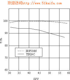
Figure 6 Relationship between power efficiency and input voltage
2.2.3 Key points of circuit design
1) Use bipolar power switch tube (VT)
(1) Select a bipolar switching tube VT that can withstand higher voltages and provide sufficient current, and its current amplification factor must be high enough.
(2) Select R14 to provide a large enough base current to ensure that the DC/DC power converter can be turned on.
(3) Select R16 (typical value is 10~20Ω) to limit the peak current generated during the switching process.
(4) It is recommended to use the TIP29C bipolar medium-power switch tube produced by Fairchild. Its main parameters are as follows: collector-emitter breakdown voltage UU (BR) CEO = 100V, maximum allowable base current IBM = 0.4A, maximum collector current ICM = 1A, maximum collector power consumption PCM = 30W, hFE = 75 times, fT = 3.0MHz.
2) Using power MOSFET (V3)
(1) R14 is selected to limit the power dissipation of Zener diodes VDZ4 and VDZ5.
(2) R15 is selected to ensure that V3 can be turned off when the input voltage is lower than 28V.
(3) Select the voltage regulation value of VDZ4 to prevent V3 from turning on when the input voltage is lower than 28V.
(4) Note that the resistance values of R14 and R15 also affect the loss of VDZ4.
(5) Select the voltage regulation value of VDZ5 to limit the maximum gate-source voltage of V3 (typical value should be 15V).
(6) It is recommended to use the IRF530N N-channel power MOSFET produced by Philips. Its main parameters are as follows: drain-source breakdown voltage U(BR)DS=100V, maximum drain power consumption PDM=79W, drain-source on-resistance RDS(ON)=80mΩ, transconductance gFS=11S, turn-on time tON=36ns, turn-off time tOFF=12ns.
3 Conclusion
There are many types of special integrated switching power supplies, and new products such as LED driver power supplies, terrestrial digital TV broadcasting (DVB-T) power supplies and power adapters can also be designed; and the advent of the LinkSwitch series of high-efficiency constant voltage/constant current three-terminal monolithic switching power supplies, LinkSwitch-TN series and DPA-Switch series monolithic switching power supplies has created favorable conditions for the optimized design of medium and small power special switching power supplies.
Previous article:Let’s talk about a small mistake that may happen accidentally in microcontroller C language programming!
Next article:Single chip alarm clock programming
Recommended ReadingLatest update time:2024-11-16 15:56


- Popular Resources
- Popular amplifiers
-
 Wireless Sensor Network Technology and Applications (Edited by Mou Si, Yin Hong, and Su Xing)
 -
 Modern Electronic Technology Training Course (Edited by Yao Youfeng)
 -
 Modern arc welding power supply and its control
 -
 Small AC Servo Motor Control Circuit Design (by Masaru Ishijima; translated by Xue Liang and Zhu Jianjun, by Masaru Ishijima, Xue Liang, and Zhu Jianjun)
 Professor at Beihang University, dedicated to promoting microcontrollers and embedded systems for over 20 years.
- Innolux's intelligent steer-by-wire solution makes cars smarter and safer
- 8051 MCU - Parity Check
- How to efficiently balance the sensitivity of tactile sensing interfaces
- What should I do if the servo motor shakes? What causes the servo motor to shake quickly?
- 【Brushless Motor】Analysis of three-phase BLDC motor and sharing of two popular development boards
- Midea Industrial Technology's subsidiaries Clou Electronics and Hekang New Energy jointly appeared at the Munich Battery Energy Storage Exhibition and Solar Energy Exhibition
- Guoxin Sichen | Application of ferroelectric memory PB85RS2MC in power battery management, with a capacity of 2M
- Analysis of common faults of frequency converter
- In a head-on competition with Qualcomm, what kind of cockpit products has Intel come up with?
- Dalian Rongke's all-vanadium liquid flow battery energy storage equipment industrialization project has entered the sprint stage before production
- Allegro MicroSystems Introduces Advanced Magnetic and Inductive Position Sensing Solutions at Electronica 2024
- Car key in the left hand, liveness detection radar in the right hand, UWB is imperative for cars!
- After a decade of rapid development, domestic CIS has entered the market
- Aegis Dagger Battery + Thor EM-i Super Hybrid, Geely New Energy has thrown out two "king bombs"
- A brief discussion on functional safety - fault, error, and failure
- In the smart car 2.0 cycle, these core industry chains are facing major opportunities!
- The United States and Japan are developing new batteries. CATL faces challenges? How should China's new energy battery industry respond?
- Murata launches high-precision 6-axis inertial sensor for automobiles
- Ford patents pre-charge alarm to help save costs and respond to emergencies
- New real-time microcontroller system from Texas Instruments enables smarter processing in automotive and industrial applications
- Problems with ADS1220
- Why do smart water meters use disposable 17450 (or other models) disposable lithium batteries? Why not use rechargeable batteries?
- 【Development and application based on NUCLEO-F746ZG motor】15. Mathematical model - voltage equation and electromagnetic torque equation
- Playing with Zynq Serial 42——[ex61] Image Laplacian Sharpening Processing of OV5640 Camera
- Snake moving in a twisting motion
- Qorvo's leading RF solutions
- Shanghai Hangxin ACM32F070 development board + serial port
- I'm a newbie and would like to ask for the code of an electronic combination lock!
- Purgatory Legend-Generate War.pdf
- In FPGA design, timing is everything

 Wireless Sensor Network Technology and Applications (Edited by Mou Si, Yin Hong, and Su Xing)


 京公网安备 11010802033920号