AD9833 is a programmable waveform generator that can generate sine wave, triangle wave and square wave output. Waveform generators are widely used in various measurement, excitation and time domain response fields. AD9833 does not require external components. The output frequency and phase can be programmed by software and are easy to adjust. The frequency register is 28 bits. When the main frequency clock is 25MHz, the accuracy is 0.1Hz. When the main frequency clock is 1MHz, the accuracy can reach 0.004Hz.
Data can be written to AD9833 through three serial interfaces. The maximum operating frequency of these three serial ports can reach 40MHz, which is easy to be compatible with DSP and various mainstream microcontrollers. The operating voltage range of AD9833 is 2.3V-5.5V.
AD9833 also has a sleep function, which can make the unused part sleep and reduce the current consumption of this part. For example, if the AD9833 output is used as the clock source, the DAC can be put into sleep to reduce power consumption. The circuit adopts a 10-pin MSOP surface mount package and is very small.
The main features of AD9833 are as follows:
frequency and phase can be digitally programmed;
when the operating voltage is 3V, the power consumption is only 20mW;
the output frequency range is 0MHz-12.5MHz;
the frequency register is 28 bits (with a reference clock of 25MHz, the accuracy is 0.1Hz);
sine wave, triangle wave, and square wave output can be selected;
no external components are required;
3-wire SPI interface;
the temperature range is -40℃-+105℃.
2 Structure and function of AD9833
2.1 Circuit structure
AD9833 is a fully integrated DDS (Direct Digital Frequency Synthesis) circuit that only requires 1 external reference clock, 1 low-precision resistor and a decoupling capacitor to generate a sine wave of up to 12.5MHz. In addition to generating RF signals, the circuit is also widely used in various modulation and demodulation schemes. These schemes are all used in the digital field. The use of DSP technology can simplify complex modulation and demodulation algorithms and is very accurate.
The internal circuit of AD9833 mainly includes numerically controlled oscillator (NCO), frequency and phase regulator, Sine ROM, digital-to-analog converter (DAC), and voltage regulator. Its functional block diagram is shown in Figure 1.
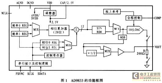
The core of AD933 is a 28-bit phase accumulator, which consists of an adder and a phase register. The phase register increases in steps for each clock. The output of the phase register is added to the phase control word and input into the address of the sine lookup table. The sine lookup table contains the digital amplitude information of a sine wave cycle, and each address corresponds to a phase point in the range of 0°-360° in the sine wave. The lookup table maps the input address phase information into a digital signal of the sine wave amplitude, and outputs the analog quantity to the DAC. The phase register returns to the initial state after every 228/M MCLK clocks, and the sine lookup table returns to the initial position after a cycle, thus outputting a sine wave. The output sine wave frequency is:
fOUT = M (fMCLK/228) (1)
Where M is the frequency control word, which is given by external programming and has a range of 0 ≤ M ≤ 228-1.
The VDD pin is used to power the analog and digital parts of AD9833, and the power supply voltage is 2.3V-5.5V. The internal digital circuit operating voltage of AD9833 is 2.5V, and the voltage regulator on the board can generate a 2.5V stable voltage from VDD. Note: If VDD is less than or equal to 2.7V, the pin CAP/2.5V should be directly connected to VDD.
2.2 Functional Description
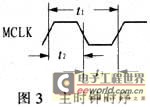
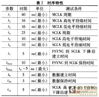
AD9833 has 3 serial interface lines, which are compatible with SPI, QSPI, MI-CROWIRE and DSP interface standards. Under the action of the serial port clock SCLK, data is loaded into the device in 16-bit mode. The timing diagram is shown in Figure 3. The FSYNC pin is an enable pin, level-triggered, and low level is valid. When performing serial data transmission, the FSYNC pin must be set low, and attention should be paid to the minimum value of the setup time t7 from the effective FSYNC to the falling edge of SCLK. After FSYNC is set low, the data is sent to the input shift register of AD9833 at the falling edge of 16 SCLKs. FSYNC can be set high at the falling edge of the 16th SCLK, but attention should be paid to the minimum and maximum values of the data holding time ts from the falling edge of SCLK to the rising edge of FSYNC. Of course, it is also possible to continuously load multiple 16-bit data when FSYNC is low, and set FSYNC high only at the falling edge of the 16th SCLK of the last data. Finally, it should be noted that the SCLK clock is a high-low level pulse when writing data, but when FSYNC just starts to become low (when writing data is about to start), SCLK must be high (note the parameter t11).
When the AD9833 is initialized, in order to avoid false output of the DAC, RESET must be set to 1 (RESET will not reset the frequency, phase and control registers). RESET will not be set to 0 until the configuration is completed and the output is required; the waveform can be observed at the output of the DAC 8-9 MCLK clock cycles after RESET is 0.
There is a certain response time in between when the AD9833 writes data to the output end to get a response. Each time new data is loaded to the frequency or phase register, there will be a delay of 7-8 MCLK clock cycles before the waveform at the output end changes. There is an uncertainty of 1 MCLK clock cycle because the rising edge position of MCLK is uncertain when the data is loaded into the destination register.
3 Pin Function and Timing of AD9833
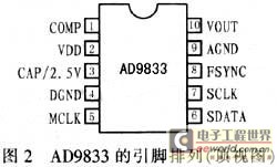
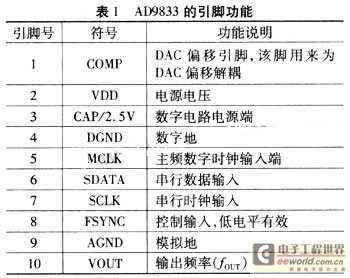
The pin arrangement of AD9833 is shown in Figure 2, and the function description of each pin is shown in Table 1.
The timing characteristics of AD9833 are shown in Figure 3, Figure 4 and Table 2.

Data can be written to AD9833 through three serial interfaces. The maximum operating frequency of these three serial ports can reach 40MHz, which is easy to be compatible with DSP and various mainstream microcontrollers. The operating voltage range of AD9833 is 2.3V-5.5V.
AD9833 also has a sleep function, which can make the unused part sleep and reduce the current consumption of this part. For example, if the AD9833 output is used as the clock source, the DAC can be put into sleep to reduce power consumption. The circuit adopts a 10-pin MSOP surface mount package and is very small.
The main features of AD9833 are as follows:
frequency and phase can be digitally programmed;
when the operating voltage is 3V, the power consumption is only 20mW;
the output frequency range is 0MHz-12.5MHz;
the frequency register is 28 bits (with a reference clock of 25MHz, the accuracy is 0.1Hz);
sine wave, triangle wave, and square wave output can be selected;
no external components are required;
3-wire SPI interface;
the temperature range is -40℃-+105℃.
2 Structure and function of AD9833
2.1 Circuit structure
AD9833 is a fully integrated DDS (Direct Digital Frequency Synthesis) circuit that only requires 1 external reference clock, 1 low-precision resistor and a decoupling capacitor to generate a sine wave of up to 12.5MHz. In addition to generating RF signals, the circuit is also widely used in various modulation and demodulation schemes. These schemes are all used in the digital field. The use of DSP technology can simplify complex modulation and demodulation algorithms and is very accurate.
The internal circuit of AD9833 mainly includes numerically controlled oscillator (NCO), frequency and phase regulator, Sine ROM, digital-to-analog converter (DAC), and voltage regulator. Its functional block diagram is shown in Figure 1.

The core of AD933 is a 28-bit phase accumulator, which consists of an adder and a phase register. The phase register increases in steps for each clock. The output of the phase register is added to the phase control word and input into the address of the sine lookup table. The sine lookup table contains the digital amplitude information of a sine wave cycle, and each address corresponds to a phase point in the range of 0°-360° in the sine wave. The lookup table maps the input address phase information into a digital signal of the sine wave amplitude, and outputs the analog quantity to the DAC. The phase register returns to the initial state after every 228/M MCLK clocks, and the sine lookup table returns to the initial position after a cycle, thus outputting a sine wave. The output sine wave frequency is:
fOUT = M (fMCLK/228) (1)
Where M is the frequency control word, which is given by external programming and has a range of 0 ≤ M ≤ 228-1.
The VDD pin is used to power the analog and digital parts of AD9833, and the power supply voltage is 2.3V-5.5V. The internal digital circuit operating voltage of AD9833 is 2.5V, and the voltage regulator on the board can generate a 2.5V stable voltage from VDD. Note: If VDD is less than or equal to 2.7V, the pin CAP/2.5V should be directly connected to VDD.
2.2 Functional Description
AD9833 has 3 serial interface lines, which are compatible with SPI, QSPI, MI-CROWIRE and DSP interface standards. Under the action of the serial port clock SCLK, data is loaded into the device in 16-bit mode. The timing diagram is shown in Figure 3. The FSYNC pin is an enable pin, level-triggered, and low level is valid. When performing serial data transmission, the FSYNC pin must be set low, and attention should be paid to the minimum value of the setup time t7 from the effective FSYNC to the falling edge of SCLK. After FSYNC is set low, the data is sent to the input shift register of AD9833 at the falling edge of 16 SCLKs. FSYNC can be set high at the falling edge of the 16th SCLK, but attention should be paid to the minimum and maximum values of the data holding time ts from the falling edge of SCLK to the rising edge of FSYNC. Of course, it is also possible to continuously load multiple 16-bit data when FSYNC is low, and set FSYNC high only at the falling edge of the 16th SCLK of the last data. Finally, it should be noted that the SCLK clock is a high-low level pulse when writing data, but when FSYNC just starts to become low (when writing data is about to start), SCLK must be high (note the parameter t11).
When the AD9833 is initialized, in order to avoid false output of the DAC, RESET must be set to 1 (RESET will not reset the frequency, phase and control registers). RESET will not be set to 0 until the configuration is completed and the output is required; the waveform can be observed at the output of the DAC 8-9 MCLK clock cycles after RESET is 0.
There is a certain response time in between when the AD9833 writes data to the output end to get a response. Each time new data is loaded to the frequency or phase register, there will be a delay of 7-8 MCLK clock cycles before the waveform at the output end changes. There is an uncertainty of 1 MCLK clock cycle because the rising edge position of MCLK is uncertain when the data is loaded into the destination register.
3 Pin Function and Timing of AD9833
The pin arrangement of AD9833 is shown in Figure 2, and the function description of each pin is shown in Table 1.


The timing characteristics of AD9833 are shown in Figure 3, Figure 4 and Table 2.


4 Internal register functions of AD9833
AD9833 has 5 programmable registers, including 3 16-bit control registers, 2 28-bit frequency registers and 2 12-bit phase registers.
4.1 Control register
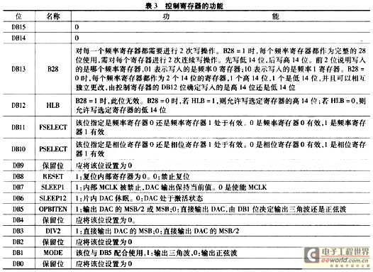
The 16-bit control register in AD9833 allows users to set the required functions. Except for the mode selection bit, all other control bits are read and acted by AD9833 at the falling edge of the internal clock MCLK. Table 3 shows the functions of each bit of the control register. To change the content of the AD9833 control register, bits D15 and D14 must be 0.
4.2 Frequency register and phase register
AD9833 contains 2 frequency registers and 2 phase registers. Its analog output is
fMCLK/228×FREQEG (2)
Where: FREQEG is the frequency word in the selected frequency register. The signal will be phase shifted:
2π/4096×PHASEREC (3)
Where PHASEREC is the phase word in the selected phase register.
The operation of the frequency and phase registers is shown in Table 4.

5 Application Design
AD9833 can be used in the detection box of the L15 aircraft control box. AD9833 is used to generate a frequency-adjustable sine wave to simulate the speed signal of the wheel speed sensor, so as to detect whether the brake anti-skid channel of the control box can brake and anti-skid normally.
5.1 Hardware circuit connection of AD9833
The detection box design uses TI's TMS320LF2407A DSP as the core controller. Two speed signals are required in the application, so the detection box needs to provide two independently adjustable frequencies. Figure 5 shows the hardware connection between TMS320LF2407A and AD9833.
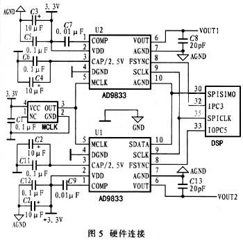
The output of the external active crystal oscillator is sent to two AD9833 as the main frequency clock. The SPI port of the DSP adopts the active working mode, that is, the SPISIMO port is used to send data. In order to match the timing of AD9833, the interface clock (SPICLK signal) mode of the DSP selects the delayed falling edge. IOPC3 and IOPC5 are used as circuit selection signals. When IOPC3 is low, U2 is selected. At this time, writing data to U1 is invalid; similarly, when IOPC53 is low, U1 is selected. At this time, writing data to U2 is invalid.
5.2 Software Program
Figure 6 shows the software flow of AD9833.
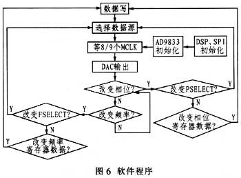
Whether writing control registers, frequency registers or phase registers, the selection signal needs to be set to the valid state before writing data, so that the written data will be valid, otherwise it will be invalid. After the DSP sends a data word, an SPI interrupt request will be generated. The interrupt mode is not used in this design, and it jumps out by querying the interrupt flag, and the DSP's receiving buffer is virtually read to clear the interrupt flag.
AD9833 has 5 programmable registers, including 3 16-bit control registers, 2 28-bit frequency registers and 2 12-bit phase registers.
4.1 Control register
The 16-bit control register in AD9833 allows users to set the required functions. Except for the mode selection bit, all other control bits are read and acted by AD9833 at the falling edge of the internal clock MCLK. Table 3 shows the functions of each bit of the control register. To change the content of the AD9833 control register, bits D15 and D14 must be 0.
4.2 Frequency register and phase register
AD9833 contains 2 frequency registers and 2 phase registers. Its analog output is
fMCLK/228×FREQEG (2)
Where: FREQEG is the frequency word in the selected frequency register. The signal will be phase shifted:
2π/4096×PHASEREC (3)
Where PHASEREC is the phase word in the selected phase register.
The operation of the frequency and phase registers is shown in Table 4.


5 Application Design
AD9833 can be used in the detection box of the L15 aircraft control box. AD9833 is used to generate a frequency-adjustable sine wave to simulate the speed signal of the wheel speed sensor, so as to detect whether the brake anti-skid channel of the control box can brake and anti-skid normally.
5.1 Hardware circuit connection of AD9833
The detection box design uses TI's TMS320LF2407A DSP as the core controller. Two speed signals are required in the application, so the detection box needs to provide two independently adjustable frequencies. Figure 5 shows the hardware connection between TMS320LF2407A and AD9833.

The output of the external active crystal oscillator is sent to two AD9833 as the main frequency clock. The SPI port of the DSP adopts the active working mode, that is, the SPISIMO port is used to send data. In order to match the timing of AD9833, the interface clock (SPICLK signal) mode of the DSP selects the delayed falling edge. IOPC3 and IOPC5 are used as circuit selection signals. When IOPC3 is low, U2 is selected. At this time, writing data to U1 is invalid; similarly, when IOPC53 is low, U1 is selected. At this time, writing data to U2 is invalid.
5.2 Software Program
Figure 6 shows the software flow of AD9833.

Whether writing control registers, frequency registers or phase registers, the selection signal needs to be set to the valid state before writing data, so that the written data will be valid, otherwise it will be invalid. After the DSP sends a data word, an SPI interrupt request will be generated. The interrupt mode is not used in this design, and it jumps out by querying the interrupt flag, and the DSP's receiving buffer is virtually read to clear the interrupt flag.
Previous article:Application of Matlab image enhancement and restoration technology in SEM images
Next article:Key points of ESD protection design for HDMI's high-speed TMDS lines
Recommended Content
Latest Industrial Control Articles
- Molex leverages SAP solutions to drive smart supply chain collaboration
- Pickering Launches New Future-Proof PXIe Single-Slot Controller for High-Performance Test and Measurement Applications
- CGD and Qorvo to jointly revolutionize motor control solutions
- Advanced gameplay, Harting takes your PCB board connection to a new level!
- Nidec Intelligent Motion is the first to launch an electric clutch ECU for two-wheeled vehicles
- Bosch and Tsinghua University renew cooperation agreement on artificial intelligence research to jointly promote the development of artificial intelligence in the industrial field
- GigaDevice unveils new MCU products, deeply unlocking industrial application scenarios with diversified products and solutions
- Advantech: Investing in Edge AI Innovation to Drive an Intelligent Future
- CGD and QORVO will revolutionize motor control solutions
MoreSelected Circuit Diagrams
MorePopular Articles
- Innolux's intelligent steer-by-wire solution makes cars smarter and safer
- 8051 MCU - Parity Check
- How to efficiently balance the sensitivity of tactile sensing interfaces
- What should I do if the servo motor shakes? What causes the servo motor to shake quickly?
- 【Brushless Motor】Analysis of three-phase BLDC motor and sharing of two popular development boards
- Midea Industrial Technology's subsidiaries Clou Electronics and Hekang New Energy jointly appeared at the Munich Battery Energy Storage Exhibition and Solar Energy Exhibition
- Guoxin Sichen | Application of ferroelectric memory PB85RS2MC in power battery management, with a capacity of 2M
- Analysis of common faults of frequency converter
- In a head-on competition with Qualcomm, what kind of cockpit products has Intel come up with?
- Dalian Rongke's all-vanadium liquid flow battery energy storage equipment industrialization project has entered the sprint stage before production
MoreDaily News
- Allegro MicroSystems Introduces Advanced Magnetic and Inductive Position Sensing Solutions at Electronica 2024
- Car key in the left hand, liveness detection radar in the right hand, UWB is imperative for cars!
- After a decade of rapid development, domestic CIS has entered the market
- Aegis Dagger Battery + Thor EM-i Super Hybrid, Geely New Energy has thrown out two "king bombs"
- A brief discussion on functional safety - fault, error, and failure
- In the smart car 2.0 cycle, these core industry chains are facing major opportunities!
- The United States and Japan are developing new batteries. CATL faces challenges? How should China's new energy battery industry respond?
- Murata launches high-precision 6-axis inertial sensor for automobiles
- Ford patents pre-charge alarm to help save costs and respond to emergencies
- New real-time microcontroller system from Texas Instruments enables smarter processing in automotive and industrial applications
Guess you like
- Programming example of MSP430 controlling digital tube
- Learn about C2000 32-bit microcontrollers
- Migrate ssh service to EK200-zlib-openssl-openssh
- Application Note Download | Keysight Technologies "Quickly Find and Identify Hidden Signal Errors"
- Ask a Question
- Cost less than 5 yuan, reliable single-fire power supply solution (using NP101A chip, including PDF...
- Mobile station development board TI MSP430FR5969LaunchPad is here!
- Can the STM32F103T8U6 use CAN?
- The romance and art of electronic engineers
- 【AT-START-F425 Review】Interpretation of I2C i2c_application.c

 Signal generator amplifier circuit based on AD9833
 AD9833 Data


 京公网安备 11010802033920号