Impedance mismatch is often encountered at SMT pads of AC coupling (also known as DC blocking) capacitors, board-to-board connectors, and cable-to-board connectors (such as SMA).
In the case of the AC coupling capacitor SMT pad as shown in Figure 1, a signal propagating along a PCB trace with a 100Ω differential impedance and a 5mil copper width will encounter an impedance discontinuity when it reaches an SMT pad with a wider copper (such as 30mil width for 0603 package). This phenomenon can be explained by equations (1) and (2). The increase in the cross-sectional area or width of the copper will increase the strip capacitance, which in turn brings a capacitive discontinuity to the characteristic impedance of the transmission channel, i.e., a negative surge.
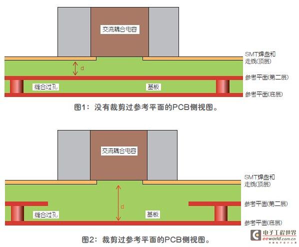
To minimize the capacitance discontinuity, the reference plane area directly under the SMT pad needs to be cut out and a copper fill is created on the inner layer, as shown in Figure 2 and Figure 3, respectively. This increases the distance between the SMT pad and its reference plane or return path, thereby reducing the capacitance discontinuity. Micro stitching vias should also be inserted to provide an electrical and physical connection between the original reference plane and the new reference copper foil on the inner layer to establish a proper signal return path and avoid EMI radiation issues.
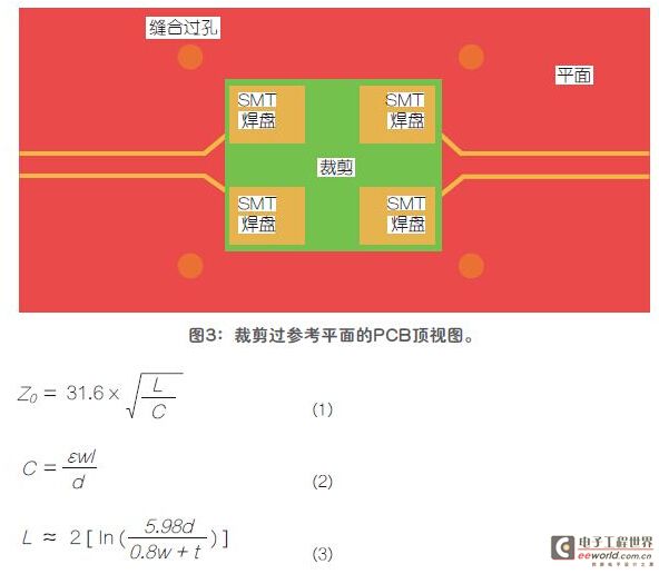
However, the distance "d" should not be increased too much, otherwise the strip inductance will exceed the strip capacitance and cause inductance discontinuity. Where:
Strip capacitance (unit: pF);
Strip inductance (unit: nH);
Characteristic impedance (unit: Ω);
ε = dielectric constant;
Pad width;
Pad length;
The distance between the pad and the reference plane below;
The thickness of the pad.
The same concept can also be applied to SMT pads for board-to-board (B2B) and cable-to-board (C2B) connectors.
The above concept will be verified by TDR and insertion loss analysis. The analysis is done by building a 3D model of the SMT pad in EMPro software and then importing it into Keysight ADS for TDR and insertion loss simulation.
Analyzing the SMT pad effect of AC coupling capacitors
A 3D model of an SMT with a medium-loss substrate is created in EMPro, where a pair of microstrip differential traces are 2 inches long and 5 mil wide, in single-ended mode, 3.5 mils away from their reference plane. The traces enter from one end of a 30 mil wide SMT pad and exit from the other end.
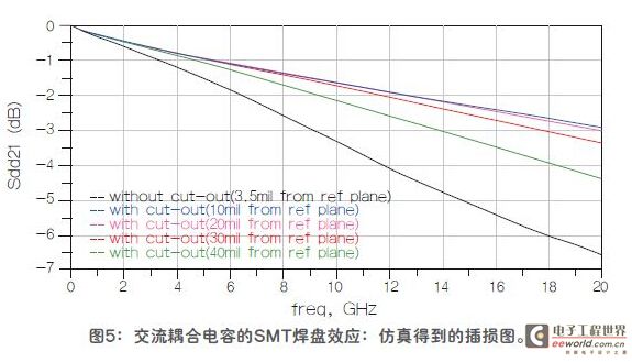
Figures 4 and 5 show the simulated TDR and insertion loss plots, respectively. The SMT design without reference plane cutouts results in an impedance mismatch of 12Ω and an insertion loss of -6.5dB at 20GHz. Once the reference plane area under the SMT pad is cutout (where “d ” is set to 10mil), the mismatch impedance is reduced to 2Ω and the insertion loss at 20GHz is reduced to -3dB. Further increasing “d ” causes the strip inductance to exceed the capacitance, resulting in an inductance discontinuity, which in turn worsens the insertion loss (i.e., -4.5dB).
Analyzing the SMT pad effect of B2B connectors
A 3D model of the SMT pad of a B2B connector is created in EMPro, where the connector pin pitch is 20 mils, the pin width is 6 mils, and the pad is connected to a pair of 5-inch long, 5-mil wide, single-ended microstrip differential traces, 3.5 mils from their reference plane. The thickness of the SMT pad is 40 mils, which is almost 40 times the thickness of the microstrip PCB trace, including the connector pins and solder.
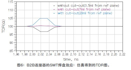
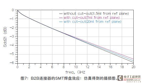
The increase in copper thickness will result in capacitance discontinuity and higher signal attenuation. This phenomenon can be seen in the TDR and insertion loss simulation graphs shown in Figure 6 and Figure 7, respectively. The impedance mismatch can be minimized by cutting out the copper area with an appropriate spacing "d" (i.e. 7mil) just below the SMT pad.
summary
The analysis in this article proves that cutting off the reference plane area directly under the SMT pad can reduce the impedance mismatch and increase the bandwidth of the transmission line. The distance between the SMT pad and the internal reference copper foil depends on the width of the SMT pad and the effective thickness of the SMT pad including the connector pin and solder. 3D modeling and simulation should be performed before the PCB is put into production to ensure that the constructed transmission channel has good signal integrity.
Previous article:How to operate a series resonant device correctly?
Next article:Itech IT7300 series programmable AC power supply in photovoltaic grid-connected inverter testing
- Popular Resources
- Popular amplifiers
- MathWorks and NXP Collaborate to Launch Model-Based Design Toolbox for Battery Management Systems
- STMicroelectronics' advanced galvanically isolated gate driver STGAP3S provides flexible protection for IGBTs and SiC MOSFETs
- New diaphragm-free solid-state lithium battery technology is launched: the distance between the positive and negative electrodes is less than 0.000001 meters
- [“Source” Observe the Autumn Series] Application and testing of the next generation of semiconductor gallium oxide device photodetectors
- 采用自主设计封装,绝缘电阻显著提高!ROHM开发出更高电压xEV系统的SiC肖特基势垒二极管
- Will GaN replace SiC? PI's disruptive 1700V InnoMux2 is here to demonstrate
- From Isolation to the Third and a Half Generation: Understanding Naxinwei's Gate Driver IC in One Article
- The appeal of 48 V technology: importance, benefits and key factors in system-level applications
- Important breakthrough in recycling of used lithium-ion batteries
- LED chemical incompatibility test to see which chemicals LEDs can be used with
- Application of ARM9 hardware coprocessor on WinCE embedded motherboard
- What are the key points for selecting rotor flowmeter?
- LM317 high power charger circuit
- A brief analysis of Embest's application and development of embedded medical devices
- Single-phase RC protection circuit
- stm32 PVD programmable voltage monitor
- Introduction and measurement of edge trigger and level trigger of 51 single chip microcomputer
- Improved design of Linux system software shell protection technology
- What to do if the ABB robot protection device stops
- Allegro MicroSystems Introduces Advanced Magnetic and Inductive Position Sensing Solutions at Electronica 2024
- Car key in the left hand, liveness detection radar in the right hand, UWB is imperative for cars!
- After a decade of rapid development, domestic CIS has entered the market
- Aegis Dagger Battery + Thor EM-i Super Hybrid, Geely New Energy has thrown out two "king bombs"
- A brief discussion on functional safety - fault, error, and failure
- In the smart car 2.0 cycle, these core industry chains are facing major opportunities!
- The United States and Japan are developing new batteries. CATL faces challenges? How should China's new energy battery industry respond?
- Murata launches high-precision 6-axis inertial sensor for automobiles
- Ford patents pre-charge alarm to help save costs and respond to emergencies
- New real-time microcontroller system from Texas Instruments enables smarter processing in automotive and industrial applications
- Free review: Domestic FPGA Anlu SparkRoad development board
- Replaying MicroPython on STM32F7DISC - DCExpert
- Problems in PCB design
- Please share the installation package of modelsim10.4 or other versions
- ATE1133 audio decoding solution, USB sound card solution, TYPE C audio adapter chip solution
- What kind of LCD screen is suitable for use in a vibration environment
- Baobaobao~~~After the Chinese New Year, what new developments are there in the evaluation industry? Hurry up and take a look at the Evaluation Intelligence Bureau~
- [NUCLEO-L552ZE Review] Small thermometer
- STM3L4R5 driver for hts221 and stts751
- Cytech’s award-winning live broadcast: Let you learn about ADI’s digital health biosensor series live!

 AWT6109M5P8


 京公网安备 11010802033920号