In addition, in order to meet the needs of actual production and power saving, LEDs usually need to be dimmed. The implementation of dimming circuits not only saves energy and reduces waste, but also prevents LEDs from working under overload for a long time, thereby improving the operating efficiency and life of LEDs. This paper studies power electronic switch converters and dimming strategies, analyzes and designs the operating status of LEDs under different dimming modes, and implements an efficient combined dimming strategy.
1 Flyback drive circuit analysis
The isolated flyback circuit has the advantages of minimum components, low cost, high power density, electrical isolation, easy multi-channel output, and voltage protection. It is suitable for low-power power supply devices below 150 W, while LED lighting generally uses low-power power supply devices. This article uses the flyback circuit as the main circuit and UC3842 as the control chip. UC3842 is a fixed-frequency current-type control chip with few peripheral components, a maximum oscillation frequency of 500 kHz, simple control, and relatively mature peripheral circuits. The circuit schematic is shown in Figure 1.
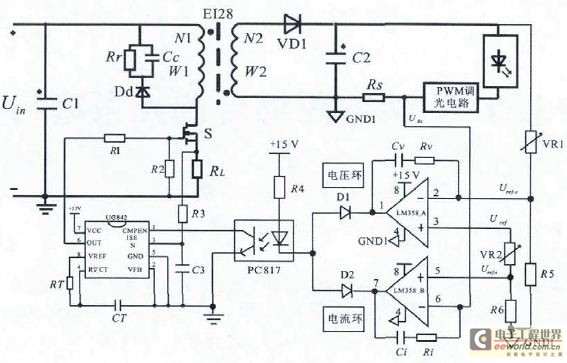
Figure 1 Flyback constant current drive circuit
LEDs are generally driven by constant current due to their steep volt-ampere characteristics. This article uses dual-loop control for constant current output. As shown in Figure 1, the current signal is converted into a voltage signal through the current sampling resistor Rs, compared with the given Uref-i value, and PI regulation is used to form a current error signal through optocoupler isolation as the given value of the inner current loop, which is compared with the switch current, and then a PWM wave is formed through the internal comparator of UC3842 to control the opening and closing of the switch tube. When the current reference value is constant, the circuit reaches a steady state, that is, a constant current output. The Uref-i value can be changed by adjusting VR2, thereby achieving a dimming effect. In addition, in order to prevent output overvoltage, a voltage loop is added to the feedback link, and the output voltage limit value is changed by adjusting VR1. In the figure, the reference voltage Uref is provided by TL431 with a reference voltage of 2.5 V.
2 Dimming Strategy Analysis
The brightness of an LED changes approximately in proportion to the change in the forward current IF. When the average forward current is changed, the light output can be changed accordingly. There are two common ways to change the IF, as shown in Figure 2.
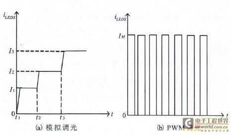
Figure 2 Two ways to change the forward current
In Figure 2(a), the luminous flux output is changed by continuously adjusting the current flowing through the LED at different times, and the current flowing through the LED is continuous; in Figure 2(b), an Im value is given first, and the current is controlled by giving different duty ratios Ddim, then the current flowing through the LED is:

Where, Ton is the conduction time of the dimming switch tube in one cycle Tdim. In this way, the dimming effect can be achieved by adjusting the dimming duty cycle Ddim and Im.
Depending on the way of changing the current, the dimming circuit can be divided into analog dimming and PWM dimming.
2.1 Analog dimming
Analog dimming methods can be divided into switch-type amplitude change AM dimming and linear dimming. The circuit control principle diagram is shown in Figure 3. Amplitude change dimming is shown in Figure 3(a). There are generally two methods:
① The reference voltage Uref-i is fixed, and the sampling resistor Rs is changed. In order to reduce the power consumption of the system, Rs is generally taken below 1 Ω, and potentiometers of about 1 Ω are relatively rare in the market; ② The current sampling resistor remains unchanged, and the size of Uref-i is linearly changed, that is, the current reference value changes. This can not only reduce the power consumption of the resistor, but also be simple and convenient. Linear dimming is to treat the power tube working in the amplification area as a dynamic resistor, as shown in Figure 3 (b) and (c), which is divided into parallel type and series type. At this time, the main circuit works in constant voltage mode, and the circuit current is adjusted by changing the resistance value of Q1. Analog dimming can avoid the noise generated during dimming, no flickering, and is simple and convenient. However, the converter is always in a continuous working state, and the system loss is relatively large; on the other hand, during analog dimming, the optical characteristics of the LED such as color temperature and light efficiency will change with the change of current, and this method is limited in occasions with strict requirements on color temperature.
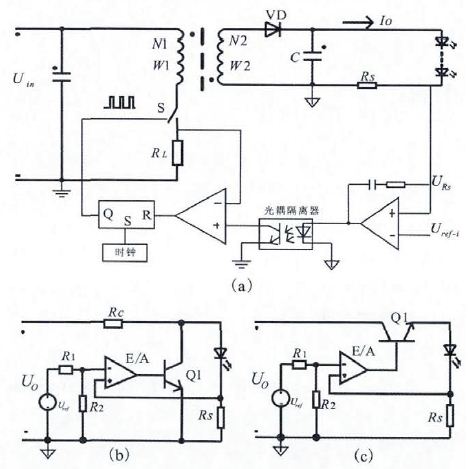
Figure 3 Schematic diagram of analog dimming
2.2 PWM Dimming
PWM dimming can accurately control the current flowing through the LED, with a wider dimming range, no color temperature drift, and high efficiency of the LED driver. The disadvantage is that it is easy to generate noise during dimming. The PWM dimming frequency is generally above 200 Hz to avoid LED flickering. The dimming scheme is shown in Figure 4. A switch tube is connected in series with the output load, and the LED current is repeatedly turned on and off by the microcontroller outputting PWM pulses to adjust the brightness of the light.
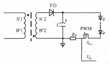
Figure 4 PWM dimming diagram
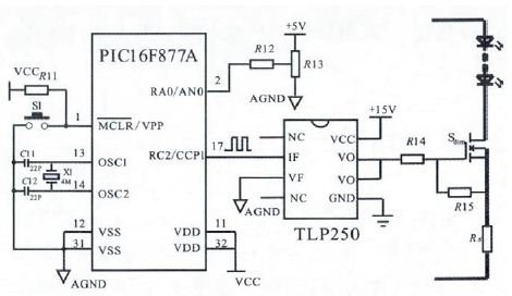
Figure 5 Schematic diagram of dimming PWM generation circuit
The PWM module is generated by the 8-bit MCU PIC16F877A produced by Microchip. The crystal oscillator of the MCU is 4 M, and the dimming frequency fdim is set to 250 Hz. The data collected by AD is converted as the given value of the duty cycle, and the PWM wave output by the MCU is amplified by TLP250 as the PWM signal to drive the dimming MOS tube. The circuit schematic is shown in Figure 5.
Since the flyback circuit cannot work in the no-load state, when the no-load state is zero, the output voltage will quickly reach the voltage limit value, so Im during PWM dimming is the maximum current of the circuit. When performing PWM dimming, first adjust the voltage loop and current loop so that the maximum operating current of the circuit is the rated current Im, and perform PWM adjustment on Im, then iLEDS=DdimIm. 2.3 Combined dimming
Combining analog dimming and PWM dimming to make up for each other's shortcomings is particularly suitable for situations where both analog dimming and PWM dimming are required. According to the circuit characteristics and practical applications, a dimming solution combining the two dimming methods is proposed.
(1) Based on PWM dimming, change Im to perform mixed dimming. When the dimming switch tube Sdim is turned off, the output voltage is the voltage limit value Uo-set. During the on-time of Sdim, the output part forms a first-order zero input response. The LED model UO=Uturn-on+Rled×IO, and the equivalent circuit diagram is shown in Figure 6. After the on-time of DdimTdim, the output voltage is:

Assume that Ddim is adjustable in the range of 0.3~1, Uo-set is 30 V, Uturn-on is 25 V, fdim is 250 Hz, output capacitance is 2000 μF, Rled is 7 Ω, then Uo>29 V. Therefore, at the moment when Sdim is turned on, Uo basically keeps the voltage limit unchanged, and the current is the maximum value Im under this limit. At this time, adjusting the current loop has no effect, and the voltage limit value is forced to change by continuously adjusting the voltage loop, thereby changing Im to achieve the dimming effect.
(2) The second dimming scheme: connect two LEDs in parallel, one using analog dimming and the other using PWM dimming. The schematic diagram of the two dimming paths is shown in Figure 7. The output voltages of paths Ⅰ and Ⅱ are both Uo, so path Ⅰ is dimmed by analog means; Im of path Ⅱ is the current value under voltage Uo, and dimming is performed by changing the duty cycle to change the current flowing through path Ⅱ. If the loads of the two paths are the same, then Io=I1+I2≈(1+D)I1.
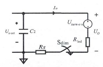
Figure 6 Output equivalent current when the dimming switch is closed
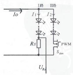
Figure 7 Schematic diagram of two-way dimming
3 Experimental Results
Based on the analysis of the above topology, a dimming circuit with input voltage Uin=36~60 VDC, output current Io=0.7 A, and output voltage Uo=30V is designed. The circuit operating frequency is 50 kHz and can dim in a wide range of 30%-100%. The load of the experiment is composed of 8 strings and 16 parallel connections of small LED lights with a rated current of 30 mA, and the maximum current can reach 1 A.
Figure 8 shows the constant current output and ripple waveforms, and Figures 9 and 10 are the driving waveforms for analog dimming and PWM dimming, respectively. Figure 11 is the efficiency curve of the three methods. It can be seen from Figure 11 that within a certain output current range, PWM dimming has the highest efficiency, followed by analog dimming, and the combined dimming efficiency is reduced, but can be maintained above 85%.
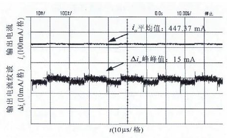
Figure 8 Output current and ripple when Uin=48 V, Io=0.45 A constant current output
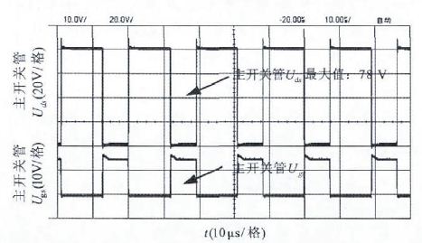
Figure 9 Uds and Ugs waveforms of the main switch tube when Uin=48 V, Io=0.45 A analog dimming
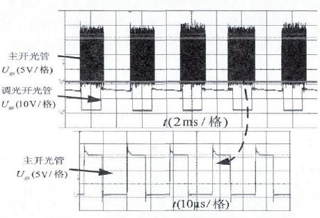
Figure 10 Ugs waveforms of the main switch and dimming switch when Uin=48 V, Io=0.45 A PWM dimming
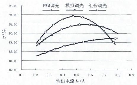
Figure 11 Efficiency comparison curve of three dimming methods
4 Conclusion
This paper adopts the flyback converter circuit topology to design an LED driver power supply and combined dimming circuit. Several LED dimming methods are analyzed and summarized. Through experimental prototype design and result analysis, the circuit realizes analog, PWM and combined dimming, with a dimming efficiency of more than 86%, a ripple of less than 4%, and a switch tube voltage stress within the allowable range, which can achieve efficient and reliable LED lighting dimming.
Previous article:High frequency and miniaturization may be the future development direction of LED switching power supply
Next article:Design of dual-Buck solar LED street light lighting control system
Recommended ReadingLatest update time:2024-11-15 15:07


- Popular Resources
- Popular amplifiers
- MathWorks and NXP Collaborate to Launch Model-Based Design Toolbox for Battery Management Systems
- STMicroelectronics' advanced galvanically isolated gate driver STGAP3S provides flexible protection for IGBTs and SiC MOSFETs
- New diaphragm-free solid-state lithium battery technology is launched: the distance between the positive and negative electrodes is less than 0.000001 meters
- [“Source” Observe the Autumn Series] Application and testing of the next generation of semiconductor gallium oxide device photodetectors
- 采用自主设计封装,绝缘电阻显著提高!ROHM开发出更高电压xEV系统的SiC肖特基势垒二极管
- Will GaN replace SiC? PI's disruptive 1700V InnoMux2 is here to demonstrate
- From Isolation to the Third and a Half Generation: Understanding Naxinwei's Gate Driver IC in One Article
- The appeal of 48 V technology: importance, benefits and key factors in system-level applications
- Important breakthrough in recycling of used lithium-ion batteries
- LED chemical incompatibility test to see which chemicals LEDs can be used with
- Application of ARM9 hardware coprocessor on WinCE embedded motherboard
- What are the key points for selecting rotor flowmeter?
- LM317 high power charger circuit
- A brief analysis of Embest's application and development of embedded medical devices
- Single-phase RC protection circuit
- stm32 PVD programmable voltage monitor
- Introduction and measurement of edge trigger and level trigger of 51 single chip microcomputer
- Improved design of Linux system software shell protection technology
- What to do if the ABB robot protection device stops
- Analysis of the application of several common contact parts in high-voltage connectors of new energy vehicles
- Wiring harness durability test and contact voltage drop test method
- From probes to power supplies, Tektronix is leading the way in comprehensive innovation in power electronics testing
- From probes to power supplies, Tektronix is leading the way in comprehensive innovation in power electronics testing
- Sn-doped CuO nanostructure-based ethanol gas sensor for real-time drunk driving detection in vehicles
- Design considerations for automotive battery wiring harness
- Do you know all the various motors commonly used in automotive electronics?
- What are the functions of the Internet of Vehicles? What are the uses and benefits of the Internet of Vehicles?
- Power Inverter - A critical safety system for electric vehicles
- Analysis of the information security mechanism of AUTOSAR, the automotive embedded software framework
- Is the STM32 library function HAL_UART_Receive blocking?
- 【DIY Creative LED V2】Complete program
- The Engineer's Way of Quanhui, the author of "FPGA Timing Constraints and Analysis"
- ALTERA cyclone V sockit development board for sale at low price and can be exchanged for E coins
- GD32L233C-START Review——04. Comparison between analog IIC and hardware IIC driving OLED
- What is the driving voltage in LCD segment code screen?
- [Smart Cup Holder] 04-Add hardware support for TouchGFX interface
- [RVB2601 Creative Application Development] RVB2601 Development Board - W800 Module Firmware Update Method
- Op amp positive and negative power supply problem
- When using FIFO to send interrupt, how to configure FIFO depth in DSP SCI?

 Siemens PLC Project Tutorial
 LED Cube Code
 ESP32-S3 source code


 京公网安备 11010802033920号