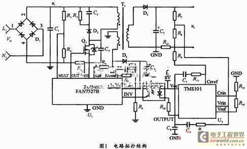
The voltage on C1 in the figure is the voltage after bridge rectification. Rs1 samples the current flowing through the MOS tube and performs cycle-by-cycle current limiting control to prevent the current peak of the MOS tube from being too large, ensuring that the transformer does not experience magnetic saturation when the load is short-circuited. The auxiliary winding is used to complete the current zero-crossing detection of the primary winding of the transformer (APFC transformer demagnetization), and the power switch tube Q2 is controlled to restart the next switch conduction working cycle. The resistance value of the resistor R4 connected to the Idet pin of FAN7527B is within the range of tens of kilo-ohms, so that the circuit works in the "quasi-zero voltage conduction" working mode.
The resistance value of R4 is related to the inductance of the primary winding of the transformer and the output capacitance of the power switch MOSFET. The specific resistance value can be determined through experiments. In this circuit, the value is 33K. Rs2 samples the load LED current signal, and R7 and R8 form a voltage divider network to sample the voltage on the LED.
Rs2 samples the current on the LED and compares it with the reference signal CVin on TM101. The output is controlled by the error amplifier for constant current. The brightness of the LED is basically proportional to the current flowing through the LED. The brightness of the LED can be adjusted by controlling the current flowing through the LED.
R7 and R8 sample the voltage on the LED and compare it with the reference signal CVin on TM101. The output voltage is controlled by the error amplifier. The two signals sent to TM101 are "ANDed" and sent to the error amplifier of the control chip FAN7527B through the optical coupler and enter the multiplier.
The other path of the multiplier is to sample the full-wave rectified mains signal through R13, R19, R23 and R27. The product of these two signals is the multiplier output. This output signal makes the inductor current track the output waveform signal of the multiplier. The generated PWM pulse controls the switch of the MOS tube Q1 to control the load current and input current, and complete the constant current and voltage limiting control of the LED and the correction of the input power factor. The LED driver power supply circuit using the flyback topology:

Previous article:LED driver design differences for different market requirements
Next article:LED backlight driving: current capability and current balance are crucial
- Popular Resources
- Popular amplifiers
- MathWorks and NXP Collaborate to Launch Model-Based Design Toolbox for Battery Management Systems
- STMicroelectronics' advanced galvanically isolated gate driver STGAP3S provides flexible protection for IGBTs and SiC MOSFETs
- New diaphragm-free solid-state lithium battery technology is launched: the distance between the positive and negative electrodes is less than 0.000001 meters
- [“Source” Observe the Autumn Series] Application and testing of the next generation of semiconductor gallium oxide device photodetectors
- 采用自主设计封装,绝缘电阻显著提高!ROHM开发出更高电压xEV系统的SiC肖特基势垒二极管
- Will GaN replace SiC? PI's disruptive 1700V InnoMux2 is here to demonstrate
- From Isolation to the Third and a Half Generation: Understanding Naxinwei's Gate Driver IC in One Article
- The appeal of 48 V technology: importance, benefits and key factors in system-level applications
- Important breakthrough in recycling of used lithium-ion batteries
- LED chemical incompatibility test to see which chemicals LEDs can be used with
- Application of ARM9 hardware coprocessor on WinCE embedded motherboard
- What are the key points for selecting rotor flowmeter?
- LM317 high power charger circuit
- A brief analysis of Embest's application and development of embedded medical devices
- Single-phase RC protection circuit
- stm32 PVD programmable voltage monitor
- Introduction and measurement of edge trigger and level trigger of 51 single chip microcomputer
- Improved design of Linux system software shell protection technology
- What to do if the ABB robot protection device stops
- Detailed explanation of intelligent car body perception system
- How to solve the problem that the servo drive is not enabled
- Why does the servo drive not power on?
- What point should I connect to when the servo is turned on?
- How to turn on the internal enable of Panasonic servo drive?
- What is the rigidity setting of Panasonic servo drive?
- How to change the inertia ratio of Panasonic servo drive
- What is the inertia ratio of the servo motor?
- Is it better for the motor to have a large or small moment of inertia?
- What is the difference between low inertia and high inertia of servo motors?
- Portable variable step-size stochastic resonance instrument based on SoC and FPGA
- Will the GaN RF market be big?
- Help
- ODX-based diagnostic application software INTEWORK-OBT
- Share the MSP430F5529 clock UCS programming considerations
- RK3288 Information
- FFT based on C2000 series DSP
- Occupy the posting position, ESP32---WS2812 16*16 dot matrix drawing points, lines and surfaces
- About the pitfalls of ADXL362 accelerometer
- SimpleLink Wi-Fi Devices

 LH0022H/883B


 京公网安备 11010802033920号