Part 1 of this article is dedicated to the theoretical analysis of a boost converter driving an LED string. This research was motivated by the need to stabilize the backlight driver loop for automotive applications. Since pulse width modulation (PWM) is used for dimming control, loop control is an important design consideration that affects the final performance. Part 2 presents the applied solution and will compare and verify the measured frequency response with the theoretically derived values.
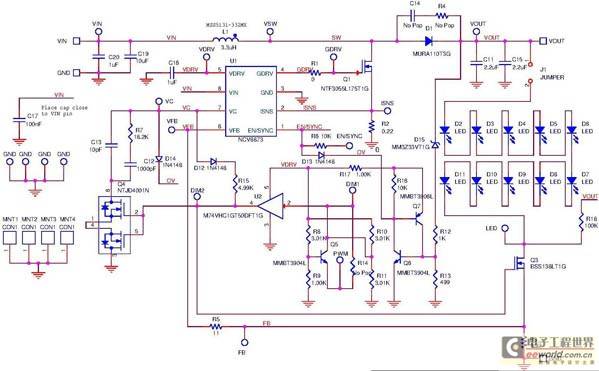
LED dimming control system circuit diagram
Analog dimming of high-brightness white LEDs will produce color shift. PWM digital dimming control is the preferred dimming method to prevent color shift because the luminous intensity will be the average lumen intensity. The LED current amplitude during the PWM conduction period is independent of the dimming ratio.
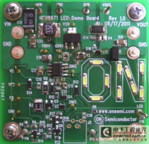
Figure 1 shows an automotive LED dimming control system that consumes less than 10 µA of quiescent current in off mode. It uses ON Semiconductor’s NCV887300[1] 1 MHz non-synchronous boost controller, which operates in constant frequency discontinuous peak current mode. The load consists of a string of 10 Nichia NSSW157-AT[2] white high-brightness LEDs connected in series. The corresponding circuit board is shown in Figure 2.
Figure 2: The NCV887300 LED demonstration board.
For ease of analysis, the key parameters of the NCV887300 controller are listed below:
- Quiescent current (Iq) < 6 µA at VIN = 13.2 V (-40 °C < TJ < 125 °C).
- EN/SYNC pin: Can be connected to external TTL instructions. The pin has dual functionality and also supports oscillator synchronization to an external clock
- ISNS: Boost transistor current sense current limit threshold voltage is 400 mV; internal slope compensation is 130 mV/µs.
- VC: Internal Operational Transconductance Amplifier (OTA) compensation pin. There is a die-level 542W ESD shunt protection resistor between the package pin and the amplifier output. The typical transconductance gm is 1.2 mS. The OTA provides 100 µA sink/source current capability.
- VFB: LED current sensing resistor R29 is adjusted according to the internal reference voltage of about 200mV.
The design goal and working principle of the LED PWM dimming control circuit shown in Figure 1 are as follows. Design Goal
Over the 6 to 18V input voltage operating range, this circuit supports a 1000:1 PWM dimming ratio at 200 Hz PWM dimming frequency, resulting in a calculated minimum pulse width of 5 µs. Operating at 1 MHz, the NCV887300 can generate a minimum of five boost transistor gate pulses to maintain the output capacitor charge to the LED current. A discontinuous conduction mode (DCM) boost topology is required to maintain regulation because the boost inductor energy is fully discharged after each gate pulse. A continuous conduction mode (CCM) topology results in poor regulation and undesirable analog dimming because the boost inductor energy buildup inertia requires several duty cycles.
Output leakage current losses must be minimized to help maintain the output capacitor charge during deep dimming operation. Leakage current causes some output voltage discharge during the LED PWM off-time, which in turn produces some analog dimming, causing significant errors in the compensation network when the PWM resumes on-time.
- Schottky rectifiers suffer from large temperature-dependent leakage currents. To minimize the boost rectifier leakage current, a boost rectifier based on ultrafast technology was selected for the circuit.
- Ceramic capacitors have much lower leakage current than electrolytic capacitors and are the preferred output boost capacitors.
- Output overvoltage monitoring circuit current consumption must be kept to a minimum. Monitoring circuits using a resistor divider network to ground are not suitable. A Zener-activated overvoltage detection circuit was chosen for this circuit because the Zener knee voltage is much higher than the battery voltage and the leakage current is very low.
Circuit operation information
Q18 blocks digital current for PWM digital dimming control. When the PWM command is active low, D34 clamps the IC's VFB feedback control voltage to a value below the controller regulation point and blocks the boost IC GDRV FET gate drive signal. Q15 is used as a compensation network state sampling/maintaining function for deep dimming applications. The universal compensation network is disconnected during PWM dimming, the feedback compensation capacitor charge (C31 and C32) is maintained, and fast dynamic control is restored when the PWM command becomes active high.
Q14 together with R48/R49/R51/R52 is used to level shift the 1.8 V logic PWM dimming signal, and U7 buffers the PWM signal to drive the bidirectional switch Q15.
If an open LED fault event is not detected, an overvoltage operating condition will result. The current sense resistor R29 voltage feedback will be 0V, resulting in an open loop output overvoltage condition. Discrete passive components are selected in the circuit to apply the overvoltage protection function and minimize the output leakage current loss when the LED system is turned off externally. The D31 Zener diode senses the overvoltage condition and triggers a soft start (D29) of the controller IC by pulling the enable pin low, interrupting the boost switch operation (D28). Resistor R30 provides a discharge path for the output boost energy storage capacitor C22.
Removing jumper J1 will shut down the LED chain to support an external load connected between the VOUT terminal and the LED terminals.
Resistor R44 is the signal injection point for the frequency response analyzer at the VFB and FB terminals. Its presence does not affect the system loop response. By injecting the frequency response analyzer signal across R44, the control output (FB/VC terminals), amplifier (VC/VFB), and open loop gain (FB/VFB) responses in closed loop form can be measured.
LED AC dynamic impedance characteristics identification
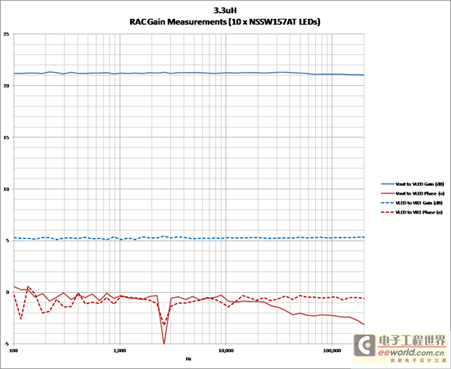
The LED dynamic impedance can be approximated based on the characteristic curves measured under specific operating conditions in the manufacturer's datasheet. The specific thermal operating conditions of the system can vary greatly. The system-level approach to system LED dynamic impedance was introduced in the Part 1 article, which characterized the device under system-level thermal conditions. For the Part 2 article, the current sense resistor, PWM FET impedance, and cumulative series dynamic impedance in the circuit were measured using a frequency response analyzer under thermally stable operating conditions of 100% PWM duty cycle (see Figure 3).
Figure 3: In-circuit small signal response of the current sensing feedback network. Closed-loop analysis
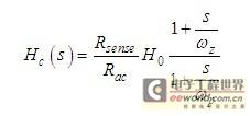
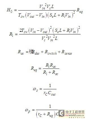
The control output (Vout) expression H(s) was derived in Part 1. Power is supplied to the LED string, but the feedback control term is the LED current sense resistor voltage VRsense (see Figure 4). The controlled system transfer function H(s) must be adjusted according to equation (1).
Figure 4. Current sensing feedback.
in:
Vc can be obtained from equation (8).
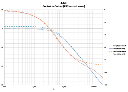
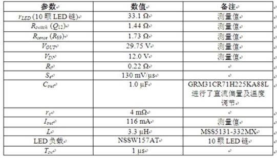
The LED dynamic impedance, series PWM transistor and current sensing resistor parameters were measured under thermally stable system-level operating conditions. VIN = 12V, Iout = 116mA are the operating parameters. The measured open-loop response Hc(s) Bode plot and measurement results are shown in Figure 5. Table 1 lists the measured parameters used to calculate the circuit diagram shown in Figure 1.
Table 1. Demo board circuit parameters
At high frequencies, the difference between the theoretical calculations and the values measured during the empirical phase becomes apparent. The difference is attributed to the lack of the RHPZ term in the numerator of the modulation transfer function of equation (1), which is described as a limitation in the simplified calculations in reference [4].
A slight difference (about 1 dB) between the theoretical and measured low frequency gain is observed. The operating losses of the boost inductor, transistor, and rectifier are neglected in the derivation of the DC operating point. If such losses were taken into account, the duty cycle DC operating point would be slightly larger, resulting in reduced low frequency gain. This can be observed by adjusting the Vin (reducing the input voltage to reduce the resistor losses) and Vout (increasing the output voltage to include the boost diode voltage drop) terms in equation (2).
System Performance
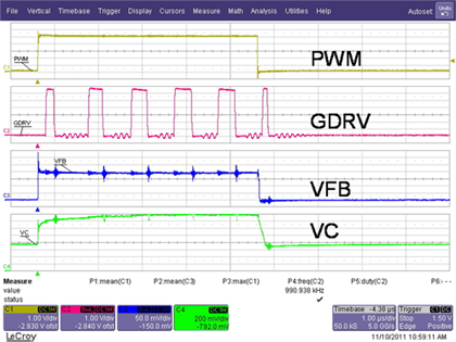
The 1000:1 200 Hz PWM dimming operating waveform of the LED dimming circuit shown in Figure 1 is shown in Figure 6. There is a small amount of compensation capacitor voltage discharge on the VC waveform, which is the result of the competition between the response time of the Q9 bidirectional switch and the activation of the PWM clamp through D19. Resistor R29 is introduced in series with the clamping diode D19 to limit the depletion of the compensation network charge. The VFB waveform maintains the desired digital waveform and amplitude (no analog dimming).
The additional short-circuit duration GDRV waveform (6th pulse) appears after the PWM signal command turns low, which is the result of the propagation delay response time of the internal logic of the NCV887300. The energy of this additional pulse is beneficial to help maintain the charge in the output boost capacitor because it compensates for some parasitic leakage current energy losses during the deep PWM dimming operating mode.
Figure 6: 1000:1 200 Hz deep dimming operation
in conclusion
The theoretical small signal response equations for a DCM boost converter driving an LED string introduced in Part 1 of this article are effectively applied to analyze an LED PWM dimming circuit in Part 2 of this article. The practical aspects of 200Hz 1000:1 deep dimming capability are explored. Simulation and measurement results are obtained for comparison with the case where phase error is neglected; phase error occurs at high frequencies due to the lack of RHPZ terms in the theoretical expression. The 1000:1200Hz PWM operating waveforms show excellent operation.
Previous article:Detailed explanation of seven commonly used and effective LED light source spectrophotometry and color separation technologies
Next article:Let's discuss how to eliminate LED flicker caused by fluctuating AC input
- Popular Resources
- Popular amplifiers
- MathWorks and NXP Collaborate to Launch Model-Based Design Toolbox for Battery Management Systems
- STMicroelectronics' advanced galvanically isolated gate driver STGAP3S provides flexible protection for IGBTs and SiC MOSFETs
- New diaphragm-free solid-state lithium battery technology is launched: the distance between the positive and negative electrodes is less than 0.000001 meters
- [“Source” Observe the Autumn Series] Application and testing of the next generation of semiconductor gallium oxide device photodetectors
- 采用自主设计封装,绝缘电阻显著提高!ROHM开发出更高电压xEV系统的SiC肖特基势垒二极管
- Will GaN replace SiC? PI's disruptive 1700V InnoMux2 is here to demonstrate
- From Isolation to the Third and a Half Generation: Understanding Naxinwei's Gate Driver IC in One Article
- The appeal of 48 V technology: importance, benefits and key factors in system-level applications
- Important breakthrough in recycling of used lithium-ion batteries
- LED chemical incompatibility test to see which chemicals LEDs can be used with
- Application of ARM9 hardware coprocessor on WinCE embedded motherboard
- What are the key points for selecting rotor flowmeter?
- LM317 high power charger circuit
- A brief analysis of Embest's application and development of embedded medical devices
- Single-phase RC protection circuit
- stm32 PVD programmable voltage monitor
- Introduction and measurement of edge trigger and level trigger of 51 single chip microcomputer
- Improved design of Linux system software shell protection technology
- What to do if the ABB robot protection device stops
- Wi-Fi 8 specification is on the way: 2.4/5/6GHz triple-band operation
- Wi-Fi 8 specification is on the way: 2.4/5/6GHz triple-band operation
- Vietnam's chip packaging and testing business is growing, and supply-side fragmentation is splitting the market
- Vietnam's chip packaging and testing business is growing, and supply-side fragmentation is splitting the market
- Three steps to govern hybrid multicloud environments
- Three steps to govern hybrid multicloud environments
- Microchip Accelerates Real-Time Edge AI Deployment with NVIDIA Holoscan Platform
- Microchip Accelerates Real-Time Edge AI Deployment with NVIDIA Holoscan Platform
- Melexis launches ultra-low power automotive contactless micro-power switch chip
- Melexis launches ultra-low power automotive contactless micro-power switch chip
- CCS import routine
- Help designing power adapter
- Seek advice from experts in lidar software and hardware
- "Playing with the Board" + Replaying MicroPython on the STM32F7DISC (6)
- Characteristics and application fields of electronic tags in various frequency bands in RFID technology
- The Hummingbird E203RISCV processor uses custom assembly instructions and NICE bus to read and write control ideas for the coprocessor memory
- [Long-term recruitment] Beijing Haidian - Annual salary starting from 600,000 - Embedded software and hardware engineer
- DIY smart car - "RoboMaster", the software framework has been open sourced
- Tube Amplifiers (4th Edition)
- Is it feasible to use a digital bridge to measure the resistance of a hygroscopic resistor to indicate humidity?



 EL5127CY


 京公网安备 11010802033920号