The luminous efficiency of LED has reached and is exceeding the level of traditional light sources such as fluorescent lamps and HID lamps, and will gradually become the mainstream light source in the field of general lighting. Due to the advantages of high light efficiency, long life, energy saving, environmental protection, and durability of LED lighting sources, LED applications and drivers have become a research hotspot in recent years. Under the same operating voltage, the forward conduction voltage drop of LEDs shows a certain difference due to the influence of process discreteness, so constant current drive is the key to white light LEDs. The best choice. The current current control methods mainly include peak current control, hysteresis control, average current control, and constant on-time control (COT) and other control methods. The mainstream peak current control has the problem of inconsistency between average current and peak current; and when the circuit duty cycle is greater than 0.5, there is a subharmonic oscillation phenomenon, and a slope compensation circuit needs to be added, which increases the circuit complexity. The average current mode can accurately control the average current, but the control method is complex to implement and still requires a slope compensation circuit. In the hysteresis current control mode, the average driving current value of the LED is determined by the internal thresholds Imax and Imin. There is no problem similar to the peak current control mode. It can better solve the shortcomings of peak current control, and no additional slope compensation circuit is required, and the circuit structure is simple. Hysteresis control has the advantages of self-stability and rapid dynamic response, and is widely used.
Some people have designed a hysteresis circuit with a simple structure and good stability, but there is no dimming circuit design. Some people have proposed a hysteresis tracking control circuit, and simulated and theoretically analyzed the circuit, but the circuit has no dimming function, and the main circuit is a traditional buck circuit, making it difficult to design a MOS tube driver. In addition, the circuit also uses a D trigger to limit the frequency jitter range, but it also limits the circuit's load capacity and the transient response becomes worse.
Based on this, this paper adopts a new step-down circuit, removes the D flip-flop, and designs an LED driver circuit with digital PWM dimming.
1 Principle and design
1.1 Working Principle
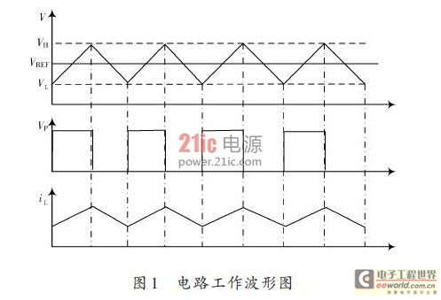
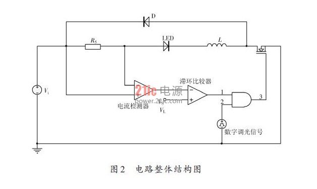
The hysteresis LED drive circuit designed in this paper consists of three parts: the main circuit, the current detection circuit, and the hysteresis control circuit. When the MOS tube is turned on, the freewheeling diode D is cut off, the current of the inductor L rises, and the voltage difference between the two ends of the sampling resistor Rs becomes larger. This voltage difference is fed back to the hysteresis control circuit through the differential amplifier circuit and compared with the threshold voltage VH or VL set by the hysteresis control circuit. As shown in Figure 1, when the voltage reaches the upper limit value VH of the voltage of the hysteresis control system, the comparator output level flips and turns off the MOS tube. Since the inductor current iL cannot change suddenly, a reverse voltage is induced at this time, and the freewheeling diode D is turned on. The inductor discharges. When the discharge voltage is lower than the lower limit VL of the voltage of the hysteresis control system, the comparator voltage flips, and the MOS tube is turned on. This cycle is repeated, limiting the peak and valley values of the inductor current, thereby achieving the control of the average value of the LED current.
1.2 Circuit Analysis The hysteresis control LED drive circuit is mainly composed of the main circuit, current detection circuit, hysteresis control circuit, and digital dimming circuit. As shown in Figure 2, the main circuit consists of RS, inductor L, freewheeling diode D, switch device MOS, and load LED. Vi is the input voltage, and RS is the detection resistor. When the circuit is stable, ignoring the conduction voltage drop of the freewheeling diode and Rs, we can get:

Where: Vi is the input voltage, Vo is the voltage across the LED, Ton is the on-time, and Toff is the off-time.
From formula (1), we can get:

The current detection circuit is a high-side current detection circuit [5-7], and the hysteresis control circuit is the core of the circuit. Some people have analyzed the current detection circuit and the hysteresis tracking circuit, and conducted simulation analysis.
By ANDing the output logic signal of the hysteresis control circuit with the digital dimming signal, a modulated PWM dimming signal can be obtained to control the conduction and cutoff of the MOS tube to achieve digital PWM dimming.
2 Experiments
2.1 Key point waveform test
Based on the above analysis, an experimental circuit is designed for verification. The circuit parameters are: RS is 0.5 Ω, the value of inductor L is 220 μH, the freewheeling diode is SS34, the switch MOS tube is IRFR024, the current detector is LM358 general-purpose operational amplifier, the comparator is LM393, the NAND gate is 74HC00, the MOS driver is UCC27524D, R1=R2=4.7 kΩ, R3=R4=47 kΩ, R7=500 Ω, R6 is three 200 Ω resistors in parallel, and R5=910 Ω.
Figure 3(a) shows the waveform of the current iRS through the LED and the gate voltage VGS of the MOS tube when the duty cycle of the experimental circuit is large. Figure 3(b) shows the waveform of the current iRS through the LED and the gate voltage VGS of the MOS tube when the duty cycle is small. Channel 1 is the current waveform through the LED measured by the current probe, and channel 2 is the gate voltage VGS waveform of the MOS tube.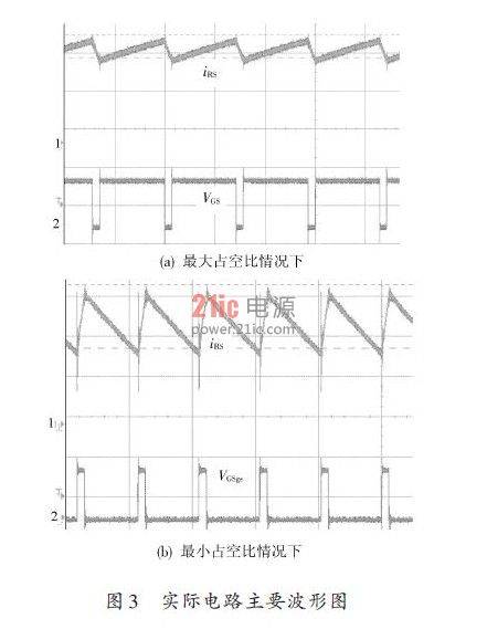
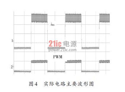
From Figure 3(a) and Figure 3(b), we can see that the iRS voltage changes hysteresis between a maximum value and a minimum value, and VGS changes between a maximum duty cycle and a minimum duty cycle. The figure shows that the hysteresis circuit can stabilize the iRS average voltage, that is, stabilize the output current Iled. And the duty cycle has a large range of variation, which can adapt to the situation where the input voltage changes or the output load changes in a large range. Figure 4 is the working waveform of the circuit when the dimming signal duty cycle is 0.5. The waveform of channel 1 is the output current waveform after the dimming signal is added. Channel 2 is a PWM digital dimming signal with a frequency of 300 Hz and a pulse width adjustable from 1% to 99%.
2.2 Experimental data testing and analysis
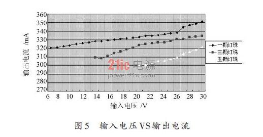
Figure 5 is a data graph showing the input voltage and output current of a circuit with 1 W, 3 W, and 5 W diodes. It can be seen from the figure that the circuit has good hysteresis control tracking performance and can stabilize the current better.
The input voltage and output current are almost linearly proportional. As the input voltage increases, the output current increases slowly. The main reason may be that the duty cycle varies widely, the stability of the feedback loop deteriorates due to changes in circuit conditions, and the inherent delay of the circuit. The average current is 360 mA from the set parameters. The actual measured result is about 330 mA, mainly because the four differential amplifier resistors of the differential amplifier circuit are not accurately matched, resulting in a difference between the amplification factor and the theoretical value. In addition, the amplification factor is also related to the amplification bandwidth of the op amp.
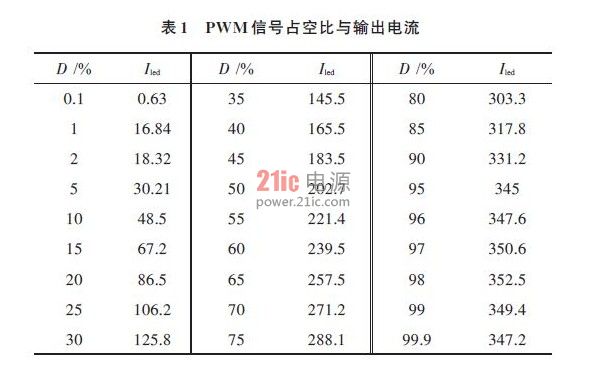
The test results in Table 1 show that under normal temperature conditions, when a lamp bead is input at 20 V, the duty cycle D of the 300 Hz PWM digital dimming signal changes from 0.1% to 99.9%. In the output current test results, the current and the duty cycle are basically linear between 5% and 95%. The dimming effect is good when the current increases by about 20 mA every 5%. Among them, when the test duty cycle is 2%~3% or 96%~99%, the current is abnormal. The main reason is that the circuit generally needs 3~4 normal switching cycles to work normally. Therefore, when the duty cycle is too small, the circuit has not worked normally and the MOS-FET gate voltage becomes low again and turns off. When the duty cycle is too large, the MOS-FET gate voltage is low, and the circuit has not been shut down normally. The next conduction time has arrived again, causing the circuit to turn on again, so the current is abnormal.
3 Conclusion
A high-side current detection hysteresis control LED drive circuit is studied and designed. The current hysteresis control method solves the problem of inconsistency between peak current and average current in current peak control, and there is no subharmonic oscillation phenomenon when the duty cycle is greater than 0.5 in peak current control, so there is no need for a slope compensation circuit, and the circuit structure is relatively simple. It can adapt to wide-range voltage input and large-range load changes. The circuit realizes digital PWM dimming. The experimental test results show that the circuit performance is stable, the dimming effect is good, there is no flicker, and the current changes smoothly. It can adapt to occasions that require intelligent dimming, meet the requirements of energy saving, and can be used in primary feedback, secondary output voltage fluctuations are large, and there is no cheap optocoupler feedback.
Previous article:A Hysteresis Control LED Driver Design
Next article:Analysis of variable mode fractional charge pump to achieve low power mobile phone LCD backlight drive solution
Recommended ReadingLatest update time:2024-11-16 19:28


- Popular Resources
- Popular amplifiers
- MathWorks and NXP Collaborate to Launch Model-Based Design Toolbox for Battery Management Systems
- STMicroelectronics' advanced galvanically isolated gate driver STGAP3S provides flexible protection for IGBTs and SiC MOSFETs
- New diaphragm-free solid-state lithium battery technology is launched: the distance between the positive and negative electrodes is less than 0.000001 meters
- [“Source” Observe the Autumn Series] Application and testing of the next generation of semiconductor gallium oxide device photodetectors
- 采用自主设计封装,绝缘电阻显著提高!ROHM开发出更高电压xEV系统的SiC肖特基势垒二极管
- Will GaN replace SiC? PI's disruptive 1700V InnoMux2 is here to demonstrate
- From Isolation to the Third and a Half Generation: Understanding Naxinwei's Gate Driver IC in One Article
- The appeal of 48 V technology: importance, benefits and key factors in system-level applications
- Important breakthrough in recycling of used lithium-ion batteries
- Innolux's intelligent steer-by-wire solution makes cars smarter and safer
- 8051 MCU - Parity Check
- How to efficiently balance the sensitivity of tactile sensing interfaces
- What should I do if the servo motor shakes? What causes the servo motor to shake quickly?
- 【Brushless Motor】Analysis of three-phase BLDC motor and sharing of two popular development boards
- Midea Industrial Technology's subsidiaries Clou Electronics and Hekang New Energy jointly appeared at the Munich Battery Energy Storage Exhibition and Solar Energy Exhibition
- Guoxin Sichen | Application of ferroelectric memory PB85RS2MC in power battery management, with a capacity of 2M
- Analysis of common faults of frequency converter
- In a head-on competition with Qualcomm, what kind of cockpit products has Intel come up with?
- Dalian Rongke's all-vanadium liquid flow battery energy storage equipment industrialization project has entered the sprint stage before production
- Allegro MicroSystems Introduces Advanced Magnetic and Inductive Position Sensing Solutions at Electronica 2024
- Car key in the left hand, liveness detection radar in the right hand, UWB is imperative for cars!
- After a decade of rapid development, domestic CIS has entered the market
- Aegis Dagger Battery + Thor EM-i Super Hybrid, Geely New Energy has thrown out two "king bombs"
- A brief discussion on functional safety - fault, error, and failure
- In the smart car 2.0 cycle, these core industry chains are facing major opportunities!
- The United States and Japan are developing new batteries. CATL faces challenges? How should China's new energy battery industry respond?
- Murata launches high-precision 6-axis inertial sensor for automobiles
- Ford patents pre-charge alarm to help save costs and respond to emergencies
- New real-time microcontroller system from Texas Instruments enables smarter processing in automotive and industrial applications
- Non-magnetic AC/DC Power Supplies
- S5PV210 Timer
- [CY8CKIT-149 PSoC 4100S Evaluation] + Create a blank project (taking Key-LED as an example)
- The difference between IPV4 and IPV6 of TCP/IP protocol
- How to set numpy floating point precision?
- EEWORLD University----[High Precision Laboratory] Sensor Technology: Temperature Sensor
- TI Award Live Pre-registration: C2000 F280013x enables lower cost and more efficient real-time control solutions
- Such an honest manufacturer is rare.
- Why does the 3.3V current not decrease after turning off the DSP peripheral clock?
- How to handle RF-PCB routing

 Siemens PLC Project Tutorial
 LED Cube Code
 ESP32-S3 source code


 京公网安备 11010802033920号