To reduce the size of the power supply while retaining the compact brick format, power supply manufacturers must reduce the height of the brick module and/or move as many external power components as possible into the brick module. However, doing both of these approaches at the same time poses many challenges to power supply designers, including how to deal with the heat dissipation required for high power density and how to integrate all the necessary components in a limited space.
To address these challenges, engineers in the Power Electronics Division of C&D Technologies (C&D) aimed to create a 600-watt brick module prototype that would save space and simplify the front-end design of 48V distributed power architecture (DPA) applications.
Silicon Carbide Semiconductors
Integrating active PFC that meets EN61000-3-2 requirements through a boost converter was a major goal of the prototype design. The difficulty of the design was that in order to keep the module height within the tolerance of the nominal half-inch high module, it was obvious that the switching frequency required would be much higher than the switching frequency typically seen in discrete PFC stages. This meant that in order for the PFC stage to meet the specifications and minimize power dissipation, a composite snubber circuit or a series of Schottky diodes would be required for protection. Unfortunately, the space required for both approaches defeats the miniaturization goal of the prototype. Fortunately, designers have found a solution in the form of the latest silicon carbide (SiC) semiconductor technology.
Electronic engineers are well aware of a law of nature: the higher the voltage rating of a device, the slower it switches. Because of this, SiC diodes (rated at 600 volts or more, easily operating at boosted supply voltages, with minimal capacitance to slow down the switching) present an almost magical solution to the problem of drastically reducing the amount of heat that would otherwise have to be dissipated by the substrate and heat sink. C&D therefore chose SiC diodes for the prototype, taking advantage of their ability to operate at very high frequencies to provide the protection it needed. The
stringent requirements for thermal performance can be mitigated by minimizing switching losses within the converter. The modular approach used in the full-bridge converter has a significant impact on the generation of losses. Understanding this problem has led to changes in the design of intermediate bus DC/DC converters, but until now, these changes have not been applied to the AC/DC conversion stage.
Low-loss topology
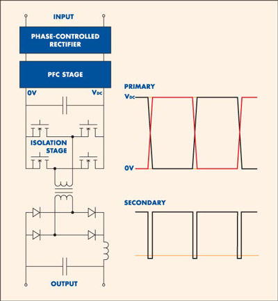
Traditionally, the quad-bridge switches are pulse-width modulated by a logic signal generated by the output voltage control signal. A slightly different technique was chosen for the prototype brick design, shown in Figure 1. This topology switches the primary side bridge switches with a constant duty cycle, allowing constant frequency operation (running at almost maximum duty cycle) with almost zero trigger voltage, thus greatly reducing switching losses.
Using this topology ensures that the output inductor is sufficiently small. When applied to a DC/DC intermediate bus converter, closed-loop regulation can be achieved by modulating the volt-seconds of the output inductor using the secondary side switch. However, the new solution does not require closed-loop regulation because the active PFC in the front end will provide a sufficiently stable 380V input to produce a fully regulated 48V DC output without the need for closed-loop control. In fact, this output is "semi-regulated", but this is sufficient because the DC/DC converter powered by the AC/DC source will itself be regulated. Running the full-bridge switch in this way results in an output post-rectifier duty cycle of around 90%, which greatly reduces the size of the output inductor. This approach is possible because the off time (during which the inductor is active) is minimized in this design.
Planar Transformers
Planar transformers are beginning to be widely recognized as an effective solution to the electromechanical problems facing power supply designers. These transformers can be made much smaller than transformers using round-section copper wire wound on traditional bobbins. Precision copper leadframes or etched windings can achieve design specifications that are much more accurate than those of wound transformers. Greater repeatability is also achieved when assembling planar transformers. An etched or stamped copper leadframe is superimposed on a flat, usually high-frequency ferrite core to create the transformer's magnetic path. This thin sheet structure also enhances magnetic coupling between the windings, resulting in low leakage inductance. The high surface area to volume ratio also makes planar magnetic components ideal for heat sink mounting and forced air cooling. As a result, very high power densities can be achieved using planar transformers.
Increasingly, DC/DC converter designers are turning to planar transformers to enhance electrical and thermal performance, as well as significantly reduce physical size, a move not often seen in AC/DC devices. However, as requirements emerged for converters with two primaries and three secondaries (and height restrictions), it became clear that C&D’s AC/DC prototype application would require a planar structure.
After confirming that planar technology was the most appropriate technology to meet the height requirements, other viable options included fully embedded transformers, embedded/standalone hybrid transformers, and fully discrete standalone transformers.
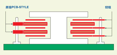
Although fully embedded transformers are space efficient and have high power density and excellent thermal performance, they are not suitable for this application because it is not possible to incorporate enough copper into their construction. Instead, C&D’s prototype module will use discrete standalone planar transformers (see Figure 2) to maximize space savings while meeting safety requirements and providing the best overall implementation cost.
Integrated Surge Control
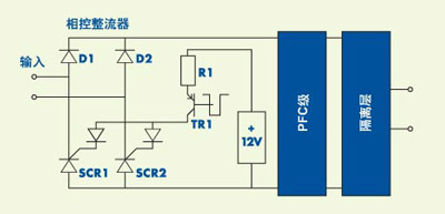
The size constraints of the prototype meant that traditional methods of limiting surges could not be used. In this case, C&D’s engineers implemented surge control using silicon-controlled rectifiers (SCRs) in place of two of the input diodes, see Figure 3. These SCRs are initially enabled just before the input voltage crosses zero, allowing a short current pulse to begin charging the bulk capacitors. Over several cycles, the activation point is gradually moved forward until it approaches the peak of the supply. This completes the surge protection process. At this point, the SCRs are activated so that they act like normal diodes, which then allows the rest of the circuit to start.
This approach also provides protection over methods such as thermistors. After a period of low load at low input voltage, an increase in load can cause a large voltage drop, causing the device to trip or become unregulated until the temperature of the thermistor rises. With the surge protection provided by the SCR design, the input voltage no longer drops in this way. With the SCR approach, surges still occur, but they are reduced to acceptable levels. This also helps with fuse selection because the effective value of the surge current is less than the steady-state current. Although the current pulse can be large (limited only by the power supply and input filter impedance), the surge rms value (a key parameter when selecting a fuse or circuit breaker) is well within the performance range of the smallest device that is likely to be used. And, because of this new surge control mechanism, the fuse can be the most common "F" type (fast-acting) of the high-blow types.
Insulated Metal Substrate (IMS)
Even assuming that above-average efficiencies can be achieved by employing efficiency-enhancing methods (such as those commonly used in DC/DC converters), our output rate and efficiency targets dictate that the prototype design must be able to dissipate up to 100 watts of heat at full load. Heat can be effectively removed from the prototype substrate by thermally coupling it to a heat sink or other heat dissipation surface. The issue here is how to transfer the heat from the components through the PCB to the substrate. In particular, it is clear that the heat dissipation requirements cannot be met using traditional FR4 PCB materials. However, an alternative, insulated metal substrate (IMS) technology (a thin dielectric layer sandwiched between the copper foil tracks and the metal substrate, as shown in Figure 4) can provide a way to meet the heat dissipation requirements.
The key technology is the dielectric material, which must provide good thermal conductivity and dielectric insulation. The limiting factor is that the substrate must provide the necessary thermal performance without making the dielectric too thin or having too much filler material. To achieve these goals, C&D selected the Thermagon 1KA T-preg IMS, which uses a dielectric with a thermal conductivity of about 4.0W/mK. The characteristics of the substrate itself are largely determined by its size and other parameters, including the thickness of the metal and the use of special techniques (such as solderable heat sinks, inner layers and thermal vias). The maximum allowable substrate temperature of C&D's prototype product is the industry de facto standard 100°C (measured by a thermocouple contacting the center of the substrate through a small hole in the heat sink). Knowing the maximum substrate size required to meet the standard brick module footprint, the metal thickness and other optimization techniques can be determined to meet the maximum allowable substrate temperature requirements.
In addition to thermal performance, there are two other reasons why Thermagon is a key choice. First, its 0.2mm insulation material has UL certification relevant to the target application; second, the technology can be used by multiple printed circuit board manufacturers that perform assembly, so the adequacy of resources can be ensured.
Reference address:Power supply design for next generation 48V distributed power architecture

To address these challenges, engineers in the Power Electronics Division of C&D Technologies (C&D) aimed to create a 600-watt brick module prototype that would save space and simplify the front-end design of 48V distributed power architecture (DPA) applications.
Silicon Carbide Semiconductors
Integrating active PFC that meets EN61000-3-2 requirements through a boost converter was a major goal of the prototype design. The difficulty of the design was that in order to keep the module height within the tolerance of the nominal half-inch high module, it was obvious that the switching frequency required would be much higher than the switching frequency typically seen in discrete PFC stages. This meant that in order for the PFC stage to meet the specifications and minimize power dissipation, a composite snubber circuit or a series of Schottky diodes would be required for protection. Unfortunately, the space required for both approaches defeats the miniaturization goal of the prototype. Fortunately, designers have found a solution in the form of the latest silicon carbide (SiC) semiconductor technology.

Electronic engineers are well aware of a law of nature: the higher the voltage rating of a device, the slower it switches. Because of this, SiC diodes (rated at 600 volts or more, easily operating at boosted supply voltages, with minimal capacitance to slow down the switching) present an almost magical solution to the problem of drastically reducing the amount of heat that would otherwise have to be dissipated by the substrate and heat sink. C&D therefore chose SiC diodes for the prototype, taking advantage of their ability to operate at very high frequencies to provide the protection it needed. The
stringent requirements for thermal performance can be mitigated by minimizing switching losses within the converter. The modular approach used in the full-bridge converter has a significant impact on the generation of losses. Understanding this problem has led to changes in the design of intermediate bus DC/DC converters, but until now, these changes have not been applied to the AC/DC conversion stage.
Low-loss topology
Traditionally, the quad-bridge switches are pulse-width modulated by a logic signal generated by the output voltage control signal. A slightly different technique was chosen for the prototype brick design, shown in Figure 1. This topology switches the primary side bridge switches with a constant duty cycle, allowing constant frequency operation (running at almost maximum duty cycle) with almost zero trigger voltage, thus greatly reducing switching losses.
Using this topology ensures that the output inductor is sufficiently small. When applied to a DC/DC intermediate bus converter, closed-loop regulation can be achieved by modulating the volt-seconds of the output inductor using the secondary side switch. However, the new solution does not require closed-loop regulation because the active PFC in the front end will provide a sufficiently stable 380V input to produce a fully regulated 48V DC output without the need for closed-loop control. In fact, this output is "semi-regulated", but this is sufficient because the DC/DC converter powered by the AC/DC source will itself be regulated. Running the full-bridge switch in this way results in an output post-rectifier duty cycle of around 90%, which greatly reduces the size of the output inductor. This approach is possible because the off time (during which the inductor is active) is minimized in this design.
Planar Transformers
Planar transformers are beginning to be widely recognized as an effective solution to the electromechanical problems facing power supply designers. These transformers can be made much smaller than transformers using round-section copper wire wound on traditional bobbins. Precision copper leadframes or etched windings can achieve design specifications that are much more accurate than those of wound transformers. Greater repeatability is also achieved when assembling planar transformers. An etched or stamped copper leadframe is superimposed on a flat, usually high-frequency ferrite core to create the transformer's magnetic path. This thin sheet structure also enhances magnetic coupling between the windings, resulting in low leakage inductance. The high surface area to volume ratio also makes planar magnetic components ideal for heat sink mounting and forced air cooling. As a result, very high power densities can be achieved using planar transformers.
Increasingly, DC/DC converter designers are turning to planar transformers to enhance electrical and thermal performance, as well as significantly reduce physical size, a move not often seen in AC/DC devices. However, as requirements emerged for converters with two primaries and three secondaries (and height restrictions), it became clear that C&D’s AC/DC prototype application would require a planar structure.

After confirming that planar technology was the most appropriate technology to meet the height requirements, other viable options included fully embedded transformers, embedded/standalone hybrid transformers, and fully discrete standalone transformers.
Although fully embedded transformers are space efficient and have high power density and excellent thermal performance, they are not suitable for this application because it is not possible to incorporate enough copper into their construction. Instead, C&D’s prototype module will use discrete standalone planar transformers (see Figure 2) to maximize space savings while meeting safety requirements and providing the best overall implementation cost.
Integrated Surge Control
The size constraints of the prototype meant that traditional methods of limiting surges could not be used. In this case, C&D’s engineers implemented surge control using silicon-controlled rectifiers (SCRs) in place of two of the input diodes, see Figure 3. These SCRs are initially enabled just before the input voltage crosses zero, allowing a short current pulse to begin charging the bulk capacitors. Over several cycles, the activation point is gradually moved forward until it approaches the peak of the supply. This completes the surge protection process. At this point, the SCRs are activated so that they act like normal diodes, which then allows the rest of the circuit to start.
This approach also provides protection over methods such as thermistors. After a period of low load at low input voltage, an increase in load can cause a large voltage drop, causing the device to trip or become unregulated until the temperature of the thermistor rises. With the surge protection provided by the SCR design, the input voltage no longer drops in this way. With the SCR approach, surges still occur, but they are reduced to acceptable levels. This also helps with fuse selection because the effective value of the surge current is less than the steady-state current. Although the current pulse can be large (limited only by the power supply and input filter impedance), the surge rms value (a key parameter when selecting a fuse or circuit breaker) is well within the performance range of the smallest device that is likely to be used. And, because of this new surge control mechanism, the fuse can be the most common "F" type (fast-acting) of the high-blow types.
Insulated Metal Substrate (IMS)
Even assuming that above-average efficiencies can be achieved by employing efficiency-enhancing methods (such as those commonly used in DC/DC converters), our output rate and efficiency targets dictate that the prototype design must be able to dissipate up to 100 watts of heat at full load. Heat can be effectively removed from the prototype substrate by thermally coupling it to a heat sink or other heat dissipation surface. The issue here is how to transfer the heat from the components through the PCB to the substrate. In particular, it is clear that the heat dissipation requirements cannot be met using traditional FR4 PCB materials. However, an alternative, insulated metal substrate (IMS) technology (a thin dielectric layer sandwiched between the copper foil tracks and the metal substrate, as shown in Figure 4) can provide a way to meet the heat dissipation requirements.
The key technology is the dielectric material, which must provide good thermal conductivity and dielectric insulation. The limiting factor is that the substrate must provide the necessary thermal performance without making the dielectric too thin or having too much filler material. To achieve these goals, C&D selected the Thermagon 1KA T-preg IMS, which uses a dielectric with a thermal conductivity of about 4.0W/mK. The characteristics of the substrate itself are largely determined by its size and other parameters, including the thickness of the metal and the use of special techniques (such as solderable heat sinks, inner layers and thermal vias). The maximum allowable substrate temperature of C&D's prototype product is the industry de facto standard 100°C (measured by a thermocouple contacting the center of the substrate through a small hole in the heat sink). Knowing the maximum substrate size required to meet the standard brick module footprint, the metal thickness and other optimization techniques can be determined to meet the maximum allowable substrate temperature requirements.
In addition to thermal performance, there are two other reasons why Thermagon is a key choice. First, its 0.2mm insulation material has UL certification relevant to the target application; second, the technology can be used by multiple printed circuit board manufacturers that perform assembly, so the adequacy of resources can be ensured.
Previous article:Monolithic Step-Down Regulator Provides On-Chip Power Sequencing for DSPs
Next article:Design of 30kHz High Frequency Switching Power Supply Transformer
- Popular Resources
- Popular amplifiers
Latest Power Management Articles
- RAQ #223: How to measure and determine soft-start timing without a soft-start equation?
- Vicor high-performance power modules enable the development of low-altitude avionics and EVTOL
- Bourns Launches Two Thick Film Resistor Series with High Power Dissipation Capabilities in Compact TO-220 and DPAK Package Designs
- Bourns Launches New High-Pulse Brake Resistor Series with Superior Energy Dissipation Capabilities
- Nexperia launches new 120 V/4 A half-bridge gate driver to further improve robustness and efficiency in industrial and automotive applications
- Vishay's New 150 V MOSFETs Offer Industry-Leading Power Loss Performance
- The first generation of SGT MOSFET series from Qiangmao: innovative trench technology, automotive-grade 60 VN channel, breakthrough in high-efficiency performance of automotive electronics
- DC/DC Power Supplies for Automotive Applications
- MathWorks and NXP Collaborate to Launch Model-Based Design Toolbox for Battery Management Systems
MoreSelected Circuit Diagrams
MorePopular Articles
- Intel promotes AI with multi-dimensional efforts in technology, application, and ecology
- ChinaJoy Qualcomm Snapdragon Theme Pavilion takes you to experience the new changes in digital entertainment in the 5G era
- Infineon's latest generation IGBT technology platform enables precise control of speed and position
- Two test methods for LED lighting life
- Don't Let Lightning Induced Surges Scare You
- Application of brushless motor controller ML4425/4426
- Easy identification of LED power supply quality
- World's first integrated photovoltaic solar system completed in Israel
- Sliding window mean filter for avr microcontroller AD conversion
- What does call mean in the detailed explanation of ABB robot programming instructions?
MoreDaily News
- STMicroelectronics discloses its 2027-2028 financial model and path to achieve its 2030 goals
- 2024 China Automotive Charging and Battery Swapping Ecosystem Conference held in Taiyuan
- State-owned enterprises team up to invest in solid-state battery giant
- The evolution of electronic and electrical architecture is accelerating
- The first! National Automotive Chip Quality Inspection Center established
- BYD releases self-developed automotive chip using 4nm process, with a running score of up to 1.15 million
- GEODNET launches GEO-PULSE, a car GPS navigation device
- Should Chinese car companies develop their own high-computing chips?
- Infineon and Siemens combine embedded automotive software platform with microcontrollers to provide the necessary functions for next-generation SDVs
- Continental launches invisible biometric sensor display to monitor passengers' vital signs
Guess you like
- [GD32E231 DIY Contest] 1. Unpacking the product
- Urgently seeking online measurement method of ground resistance of fuel dispenser
- Calculation of Frequency of Various RLC Combination Circuits
- Ultra-precision long delay circuit
- A new interpretation of the principle of integral circuits: the transformation of amplifiers and capacitors
- EEWORLD University Hall ---- Operating Systems (Xiang Yong and Chen Yu from Tsinghua University)
- Provide technical support
- High sensitivity hall sensor selection
- Gizwits Intelligent Gateway Solution enables interconnection of different brands and protocols
- We know that overvoltage may break down the load, but why do we need undervoltage protection and open circuit protection?

 PTQB425080,pdf(200-W 48-V Inpu


 京公网安备 11010802033920号