Terrible Japanese materials: causing global semiconductor panic!
In ancient times, a small village near the Yellow River built a towering dam to prevent annual floods.
One day, an old farmer suddenly discovered an ant nest on the embankment. He thought it might be unsafe, so he turned back to the village to report.
On the way, he met his son. After listening to the old farmer's story, the son said disapprovingly: " Such a solid long embankment will be afraid of a few small ants?" Then he took the old farmer to the field together.
But that night there was a storm, the river water rose sharply, the turbulent river water seeped out from the ant hole and eventually broke the dam.
If the old man in the story had a stronger sense of crisis and insisted on independent thinking, he would eventually save the vast majority of people and his elderly self.
Our country should be grateful that there is an old man like Ren Zhengfei who is decisive and forward-thinking, and who started preparing to plug the "holes" in China's semiconductor "dam" more than a decade ago.
More than a decade later, the United States shouted loudly, ZTE fell to the ground, and Huawei was still standing.
Although the light of Huawei has brought us a lot of courage and confidence, we must not relax our composure, because in addition to this "visible loophole", there are many inconspicuous ant holes that are posing hidden dangers to this "dam" that has not yet been built.
On July 1, Japan announced restrictions on its domestic companies' exports of high-purity hydrogen fluoride, photoresists, and fluorinated polyimides to South Korea. South Korean conglomerates were shocked and organized plans to go to Japan to seek solutions from Japanese suppliers.
A few days later, the South Korean government urgently dispatched senior officials to visit the United States, hoping that the United States, as the big brother, could speak for South Korea in this incident.
In addition, Japanese and South Korean officials also plan to hold talks in Japan on export restrictions.
Among the three materials restricted this time, hydrogen fluoride is highly toxic, and photoresist cannot be stored for a long time, otherwise it will easily deteriorate. Therefore, Korean companies only have a small amount of stock. Some people even pointed out that Samsung’s inventory of related raw materials is only a few weeks left.
Moreover, the restricted materials cannot be quickly replaced elsewhere.
If the negotiations fail and the restrictions continue to be implemented, the status of South Korea, a panel and memory giant, will be in jeopardy.
The three materials involved in this incident, hydrogen fluoride, photoresist, and fluorinated polyamide, have several commonalities:
Low cost, high difficulty, and extremely critical.
Whether it is hydrogen fluoride or photoresist, its cost generally accounts for single digits in the total cost of the industry, basically not exceeding 5%.
However, the time span from development to testing to application of these materials is long, the process is complex, and the overall R&D cost is high.
Most importantly, these materials are key materials that affect the quality of downstream end products.
Compared with the $400 billion semiconductor market, the $130 billion panel market, and the $60 billion printed circuit board market, the space for these three materials is only a few billion dollars, which seems insignificant.
But these tiny products are almost all monopolized by Japanese companies.
Currently, more than 90% of the world's fluorinated polyimide comes from Japanese suppliers, such as Shin-Etsu, JSR , and Sumitomo Chemical .
The world's top five manufacturers account for 87% of the photoresist market , and the industry is highly concentrated. Among them, Japan's JSR, Tokyo Ohka, Japan Shin-Etsu and Fuji Electronic Materials have a combined market share of 72%.
In the global high-purity hydrofluoric acid (hydrogen fluoride) market , Japanese companies occupy an absolute dominant position. The three Japanese companies , Ruixing Chemical, Daikin, and Morita Chemical, have a combined market share of more than 93%.
In these three raw material areas, Japan has the final say. The three arrows it fired at South Korea this time are deadly and can be said to be strangling South Korea's neck.
People outside the industry are gloating over the fight between the "Japanese" and the "Bangkok", but people inside the industry are terrified when they think about the incident carefully.
1
Among the three raw materials mentioned above, photoresist is the most critical and it is more difficult to make a breakthrough. This article will introduce the importance of photoresist to the development of China's industry.
There are three main application scenarios for photoresist: semiconductors, display panels, and PCB (printed circuit boards), and their market shares are similar, basically around 25%.
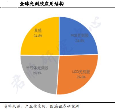
Why should we pay attention to this incident?
The reason is that China's development in the above three application areas of photoresist is in full swing.
1. China's PCB is gradually becoming the king
Friends who often read Junlin’s articles may not be unfamiliar with PCB. Junlin has a complete introduction and research on the PCB industry and companies in the industry.
The key to studying PCB is to understand China's position in the world.
According to statistics, at the beginning of this century, the PCB output value of Europe, the United States and Japan accounted for 75% of the world's total. However, today, the output value of the three regions combined is less than 20%.
China has long been the dominant player, accounting for 50% of the global market share.
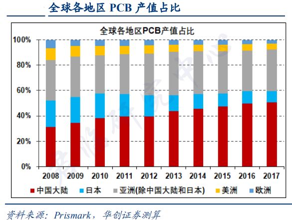
In this industry, China has advantages such as labor costs and proximity to the market, becoming a gathering place for the global PCB industry. The industry has been smoothly transferred from Europe, the United States and Japan to China.
Even the PCB industries in South Korea and Taiwan have had to be slowly absorbed by the mainland under the strong attraction of China.
For example , Pengding Holdings (002938.SZ) , a Taiwanese company and a world-class PCB giant that has served Foxconn closely, has now gone public on the A-share market, and the locations for its new production capacity are basically all in China.
It can be foreseen that the siphon effect formed by China will continue in the future driven by the 5G industrial chain, and the global share of PCB will increase, forming an oligopoly structure in the PCB industry.
2. Display panels, leaping into the first-tier camp
In 2016, China's LCD panel production capacity accounted for 25.91% of the world's total. IHS predicts that in 2017, the proportion will exceed 1/3, and it is expected to surpass South Korea to become the world's largest LCD panel production base.
In 2019, the production capacity share will exceed 40%, and is expected to exceed 50% in 2022.
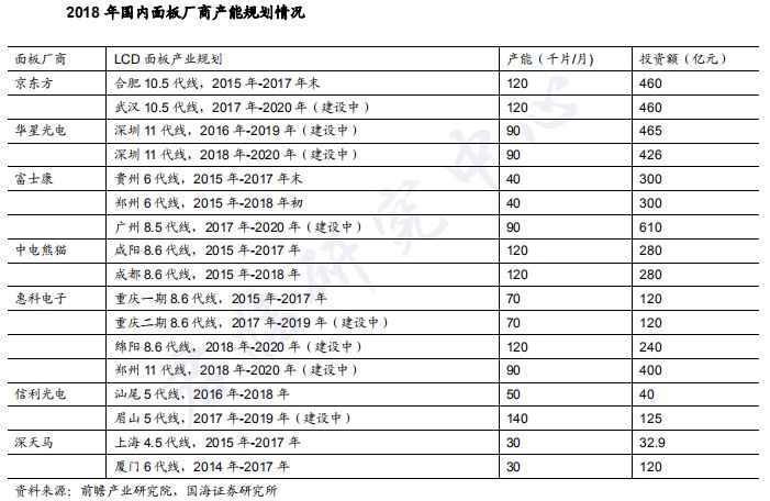
However, some investors believe that LCD is an outdated industry and may be replaced by new display panels such as OLED at any time.
However, from the perspective of terminal applications, LCD is mainly used in TVs. Although the shipment volume is not large, the application area is large, and under the trend of large screens, the application of LCD is increasing year by year.
However, due to its high cost, OLED is mainly used in small-screen mobile phones and has not yet become popular. Samsung is the main producer of OLED in the world.
There is currently no question of the two technical products replacing each other.
But then again, no matter what kind of product it is, it requires the crucial photoresist as a protective agent in the etching process, so there is no problem of the photoresist market disappearing after the product technology is updated.
Therefore, with the global panel transfer, the use of photoresist in Chinese panels will increase as panel production increases.
3. Semiconductors: Global production capacity shift
The semiconductor field is the weakest link among these three industries.
If we say that the PCB industry has won a great victory, it has almost completely taken over low-end and mid-end applications, and has fully penetrated high-end applications, forcing European, American, and Japanese companies with high-end PCB applications into a corner. The gross profit margin of their high-end products is even lower than that of our low-end and mid-end products. (It is due to labor costs and economies of scale)
The panel industry has initially laid the foundation for reaching the top. China is a major manufacturer of televisions and monitors, as well as a major exporter. This has led to the rise of a number of display panel companies, but China is slightly behind in panel technology and has not yet reached the highest level in terms of technical processing. However, it is only a matter of time before this is overcome.
Only in the semiconductor industry, the layout of the entire industry is relatively primitive. Although there are a few outstanding ones, most of them are just starting out.
The semiconductor industry is mainly based on integrated circuits, which account for more than 80% of the total. Therefore, when people talk about semiconductors, they are basically talking about integrated circuits.
The integrated circuit industry chain is divided into: raw materials and equipment - design - manufacturing - packaging and testing - downstream applications .
The further downstream the integrated circuit industry chain is, the more domestic companies there are and the more say they have; the further up the industry chain you go, the fewer influential companies there are. (Huawei is a special case in the design field)
At present, China's main advantage lies in the market demand brought about by the huge application scenarios. This is the largest market outside the United States.
Next is packaging and testing, which occupies a large share of the global low-end market and is now gradually penetrating into the mid-end market.
As for the manufacturing process, there is still a huge gap from the most advanced manufacturing technology, and we are still working on conquering the mainstream process.
The manufacturing process is mainly based on wafer foundry. After packaging and testing companies, wafer foundries will be an important step in further increasing the localization process of integrated circuits.
According to the global wafer fab forecast report released by the Semiconductor Industry International (SEMI) in the past two years, 26 new wafer fabs are expected to be put into production in the mainland in the four years from 2017 to 2020. The entire investment plan accounts for 42% of the world's new wafer fabs, making it the region with the largest new investment in the world.
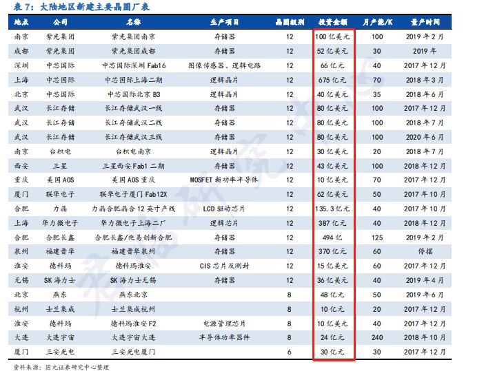
The application of photoresist in the integrated circuit industry is in the manufacturing process. The increase in the number of silicon wafer fabs in the future also means an increase in the use of photoresist. With the deepening of the industrial transfer process, China will also become the main user of integrated circuit photoresist in the future.
It seems that industrial transfer has become a trend whether it is PCB, display panel or integrated circuit, and the corresponding demand for the use of photoresist will also show a trend of growth.
However, the domestic supply of photoresist is still worrying.
In 2015, China's domestic photoresist products were mainly concentrated in low-end PCB photoresists, with a PCB photoresist market share of 94.4%;
LCD photoresist ranks second, with a market share of only 2.7%;
The semiconductor photoresist market accounts for only 1.6%, and there has not been much improvement so far.
Looking at the construction of LCD and OLED production capacity, and the establishment of silicon wafer factories one after another, this trillion-dollar investment will be difficult to operate without this "tiny" supply of photoresist.
To use an inappropriate analogy, this is equivalent to spending a lot of money to buy a high-end sports car, but being cut off from the gas supply.
Seeing Japan strangling South Korea at this moment, our generation should not just stand by and watch the fun, but should be prepared for danger in times of peace and promptly fill the "ant holes" on the magnificent dam of China's industrial transfer.
2
The development history of the world's electronics industry is also a history of industrial transfer. PCB, display panels, and semiconductors have similar experiences. They originated in the United States, matured in Japan, and were overtaken by South Korea and Taiwan in some areas. Finally, it was the turn of mainland China.
This path of industrial transfer is related to the changes of the times and the trends of technological development, the rise of the local economy, and the local government and people.
The economic rise of a region often benefits from the wave of innovation in world science and technology. Under the decision-making of the local government, the whole nation focuses on tackling emerging and high-end industries, combined with the people's desire for wealth and strong ambition, so that they can successfully cross the middle-income trap and break into the ranks of developed countries.
The development process of Japan and South Korea is so similar to that of China.
But what is strange is that this kind of industrial transfer is not comprehensive, especially in the field of key raw materials. South Korea and Taiwan can tackle the tough problems in the field of integrated circuits, but they cannot be self-sufficient in a small photoresist. Why is this?
The root cause lies in the multiple barriers to manufacturing qualified photoresists - technical barriers, financial barriers, and customer barriers.
1) Technical barriers
Since they are used for micron-level or even nano-level graphic processing, the products need to have strict quality control. Photoresists and their special chemicals have special chemical structures, high quality requirements, extremely low content of microparticles and metal ions, and complex production processes. Therefore, the technical threshold is extremely high.
For example, in the field of integrated circuits, one of the steps is to drip photoresist onto the center of a silicon wafer, and then rotate the silicon wafer at high speed so that the liquid glue in the center is evenly coated on the silicon wafer.
During this process, the thickness difference of the glue on the silicon wafer cannot exceed 5nm (nanometers). Such an extreme difference naturally requires extremely detailed requirements for the modulation of the glue.
In addition, the quality of the photoresist will affect the contrast value. The higher the contrast, the steeper the sidewalls of the formed pattern and the better the quality.
Lithography effects at different contrasts:
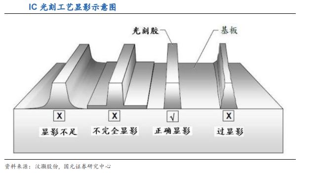
In addition, photoresist has extremely detailed requirements in terms of resolution, viscosity, sensitivity, corrosion resistance, surface tension, storage and transmission. The specific values are accurate to the nanometer level and the composition is accurate to the molecule . It can be seen how difficult it is.
The application levels of photoresists in integrated circuits are divided into ordinary broadband photoresists, g-line (436nm), i-line (365nm), KrF (248nm), ArF (193nm), F2 (157nm), and the most advanced EUV (<13.5nm) line level.
The higher the level, the higher the limit resolution, the greater the wiring density of the silicon wafer with the same area, and the better the performance.
Currently, only companies in the United States and Japan can achieve ArF technology level and above, and other regions in Asia, including China, have no mass production capabilities.
2) Capital barriers
The research and development of photoresists requires supporting lithography machines, mask plates and other processes.
You should know that the most advanced lithography machine in the world is the EUV lithography machine, which can only be manufactured by ASML of the Netherlands . An EUV lithography machine is worth $100 million and is in short supply. The price of a DUV lithography machine with a relatively poor process is also tens of millions of dollars.
Although China does not yet have the research and development capabilities for EUV and DUV photoresists, if it wants to develop more advanced photoresists, the subsequent investment will be quite large.
In addition to the supporting equipment, hiring talents also requires a lot of money. These two have common characteristics: advanced lithography equipment is extremely expensive, and the salary of high-end talents is also very high, but they are in short supply and scarce in the market.
3) Customer barriers
When the photoresist reaches the required technical level, it is necessary to contact downstream customers and conduct testing after the customers agree. This testing and verification process usually takes 2-3 years. Once cooperation is established, a long-term supply relationship will be formed, and new process technologies will be jointly developed, and the relationship will be very close.
If the cost of photoresist accounts for a large proportion of the overall cost of downstream customers, then in order to pursue efficiency, downstream customers will be more proactive in requesting testing. However, photoresist accounts for a very small proportion of the overall cost, and it takes 2-3 years for downstream customers to arrange testing. During such a long period of time, personnel tracking and production line coordination are required, and the verification cost is too high.
Moreover, downstream customers have good cooperation with their existing suppliers. The two parties have cooperated for many years and are very familiar with each other's work processes, R&D processes, etc. If they rashly cooperate with a new supplier, both parties will need to re-adjust in many areas, which will affect work efficiency.
The most important thing is that photoresist has a huge impact on the quality of the final product. If there are no special reasons, the quality can basically be guaranteed if the products of the original supplier are used.
Therefore, generally speaking, once downstream customers form a stable cooperative relationship with their original suppliers, they will continue to cooperate for a long time.
You see, photoresist technology is difficult, and development requires large capital costs, time costs, and manpower costs;
Even if the research and development is successful, downstream customers will need to go through a long period of certification and bear the corresponding costs, and will also have to bear the consequences of a series of problems caused by glue quality issues;
Since the cost of photoresist is low, it is difficult for downstream customers to make the decision to change suppliers.
Therefore, once you become a supplier to a certain company, as long as there are no problems with your own products and your research and development can keep up, you basically don't have to worry about customers "changing their minds".
On the other hand, if the products of the followers remain in the research and development and testing stages, they will face a huge gap in the future.
Because only during the application process of photoresist can problems be discovered and solved, and the technology, process and product levels can be continuously improved. Otherwise, it will remain in the laboratory and the technology will stagnate.
This is why, although South Korea and Taiwan have achieved world-leading levels in the semiconductor and other fields, they are nowhere to be seen in the field of key high-end raw materials.
In fact, with the technical level they have achieved, they are fully capable of overcoming the problem. However, because they are worried about the quality and economic benefits problems caused by using glue from domestic manufacturers, they gave up their investment and attention in this area early on.
Moreover, they naively believed that under the market economy, the government would not interfere with the operation of enterprises, and the supply of raw materials would not be hindered, so they would not need to spend huge amounts of energy on research and development.
But the facts finally proved that this was nothing more than self-promotion and beautification of the capitalist market.
From the perspective of barriers, if the research and development and application of raw materials cannot keep up, China's huge industrial transfer will eventually be restricted by others.
So to put it bluntly, it means "sticking your neck out and waiting for others to sharpen their knives"?
No.
According to United Nations survey statistics, my country has 39 major industrial categories, 191 medium categories, and 525 small categories. It is the only country in the world that has all the industrial categories in the United Nations industrial classification.
It can be said that there is almost nothing in the world that cannot be made in China, it is just a matter of quality.
The same is true for photoresist. China has low-end products in the photoresist field and has also dabbled in the research and development and production of mid-range products, but domestic downstream companies are unwilling to use them and basically rely on imports.
However, since the "sweater war", China's semiconductor industry and upstream and downstream have reached a consensus - "if domestic products can be used, try to use domestic products."
Although this has not been publicly publicized in the media, it has basically become an undisclosed consensus in the industry, judging from the annual reports of listed companies and the reactions of domestic companies after being sanctioned.
In addition, at present, domestic photoresist has made some technological breakthroughs, and downstream manufacturers are also actively arranging inspections and tests. With the passing of the tests, we will form stable cooperation with enterprises and have a stable cash flow. With the strong support of the country, we will continue to advance to the most cutting-edge technology.
3
Although there are not many domestic photoresist companies, their scale has basically reached a certain level. Let’s take stock of them below.
Feikai Materials (300398.SZ) is a professional company that researches, produces and sells materials and specialty chemicals used in high-tech manufacturing. Its core products include UV-curing materials and electronic chemical materials.
In 2016, the company's 3,500 tons/year UV-curing photoresist project was officially put into production (used in the PCB field). At the same time, the company is making arrangements in the TFT-LCD photoresist field and plans to build an annual output of 5,000 tons of TFT-LCD photoresist production line, which has basically been completed. By then, the company will have a pivotal position in the PCB and LCD photoresist fields.
Rongda Photosensitive (300576.SZ) has three product series: PCB photosensitive ink, photoresist and supporting chemicals, and special ink. The properties of photosensitive ink are similar to those of photoresist, both of which are anti-corrosion solvents.
The company is a leading domestic PCB photosensitive ink manufacturer, with an output of 12,000 tons in 2018, a year-on-year increase of 10.37%, accounting for approximately 7% of the PCB photosensitive ink market, which is the company's main product.
In terms of capacity expansion, 10,000 tons of photosensitive ink will be put into production in the first half of 2019, 700 tons of TFT-LCD positive photoresist will be completed by the end of 2020, and some semiconductor photoresist production capacity will be planned. Rongda Photosensitive will simultaneously deploy three types of photoresists: PCB, display panel, and semiconductor.
Shanghai Xinyang (300236.SZ)' s main business is semiconductor-specific chemical materials and supporting equipment. Its downstream customers are basically domestic packaging and testing companies, and it provides them with electronic cleaning and electronic electroplating products. It has only entered the photoresist field in recent years and has also deployed related equipment for semiconductor manufacturing.
The company has entered the supplier list of leading domestic companies such as SMIC, Wuxi Hynix, Huali Microelectronics, Tongfu Microelectronics, Suzhou Jingfang, and Changdian Advanced Packaging .
In order to speed up the research and development progress of photoresists and quickly seize the existing market, the company and the technical team of Dr. Deng Hai, a domestic photoresist expert and expert in the National Thousand Talents Program, jointly invested in the establishment of Shanghai Xinkewei. Shanghai Xinyang holds 80% of the shares and is the company's holding subsidiary.
Dr. Deng Hai is currently the chief scientist of the National 02 Project. He is one of the earliest people in the world to be involved in 193nm photoresist technology. He has worked in famous American semiconductor companies for many years and served as a Fellow of the semiconductor materials company Tokyo Ohka.
Shanghai Xinkewei is conducting a 193nm (ArF) dry photoresist research and development and industrialization project, which is expected to reach full production in 2022. After reaching full production, the project will have an annual production capacity of 5,000 gallons of 193nm dry photoresist and supporting materials.
Jingrui Co., Ltd. (300655.SZ) is a company specializing in microelectronic chemicals. Its products include ultra-clean high-purity reagents, photoresists, functional materials, lithium battery materials and basic chemical materials, which are widely used in semiconductors, lithium batteries, LEDs, flat panel displays and photovoltaic solar cells.
Its subsidiary Suzhou Ruihong is the earliest company in China to engage in photoresist research and large-scale production, and has undertaken the "02 Special Project", a major domestic science and technology project.
"02 Project" refers to the "Extremely Large Scale Integrated Circuit Manufacturing Technology and Complete Process" project proposed by the State Council in 2006. Because it ranks second among the 16 major national projects, it is called "02 Project" in the industry.
Currently, Suzhou Ruihong has basically completed the layout of mainstream semiconductor photoresists, and its G-line and I-line have both entered mass production. Among them, the I-line completed capacity construction last year and has achieved a scale of 100 tons/year.
We have obtained supply orders for I-line positive resist and thick film resist from SMIC Tianjin, Yangjie Technology, and Fushun Microelectronics.
At the same time, in terms of product research and development, we have completed the pilot technology research on the more technically difficult KrF (248nm) photoresist raw materials.
NCU Optoelectronics (300346.SZ) is an enterprise engaged in the research and development, production and manufacturing of various chemical materials. Its main business is high-purity metal organic compounds (MO sources). It is one of the world's leading suppliers of MO sources. The company has fully reached the international advanced level in the synthesis and preparation of MO sources, purification technology, analysis and testing, packaging containers, etc., and also laid out the electronic gas business in 2017.
The most important layout of Nanda Optoelectronics in the field of photoresist was the acquisition of 31.39% of the equity of Beijing Kehua in 2015.
Beijing Kehua was established in August 2004. It is the first company in China to produce photoresist and has built China's first modern photoresist production line with independent intellectual property rights.
Beijing Kehua's main business is only photoresist. Therefore, by focusing on its main business, it can invest a large amount of funds and personnel in research and development. Its current product line covers KrF (248nm), I-line, G-line, UV broadband and other photoresist products. It has the richest product line among its domestic peers.
At present, compared with domestic counterparts, it has the most advanced 248nm photoresist mass production line with an annual output of 10 tons. In 2018, it jointly undertook the "Extreme Ultraviolet Photoresist Materials and Laboratory Testing Technology Research" project of the "Extreme Large Scale Integrated Circuit Manufacturing Equipment and Complete Process" (02 Special Project) with the Institute of Chemistry of the Chinese Academy of Sciences and the Institute of Physical and Chemical Technology of the Chinese Academy of Sciences, and passed the national acceptance.
We have completed the design, preparation and synthesis process research of the world's most advanced EUV photoresist key materials, the formulation composition and photoresist preparation, and the development of preliminary evaluation equipment for laboratory photoresist performance.
Although Nanjing University of Science and Technology Optoelectronics withdrew from Beijing Kehua in January 2019, it carried the corresponding technical strength of Beijing Kehua. In December 2018, Nanjing University of Science and Technology Optoelectronics invested 656 million yuan to build the "193nm (ArF) Photoresist Material Development and Industrialization" project, which is expected to be put into production in three years.
In general, the company with the strongest R&D capabilities at present is Beijing Kehua, which is most likely to be the first to break the monopoly of foreign high-end photoresists in the semiconductor field. Next is Nanjing Optoelectronics, whose high-end project will be put into production in three years. Jingrui Co., Ltd. and Shanghai Xinyang both have good R&D capabilities and have R&D investments in the field of high-end photoresists.
Junlin believes that although China's mid-to-high-end photoresists are still controlled by others, with the research and development breakthroughs of domestic raw material companies and the consistent support of domestic downstream companies for domestic production, the monopoly of photoresists by foreign countries will not last long.

Focus on industry hot spots and understand the latest frontiers
Please pay attention to EEWorld electronic headlines
https://www.eeworld.com.cn/mp/wap
Copy this link to your browser or long press the QR code below to browse

The following WeChat public accounts belong to
EEWorld(www.eeworld.com.cn)
Welcome to long press the QR code to follow us!

EEWorld Subscription Account: Electronic Engineering World

EEWorld Service Account: Electronic Engineering World Welfare Club
Featured Posts


 京公网安备 11010802033920号