Basic knowledge of LDO, just read this article
▲ For more exciting content, please click the blue text above to follow us!
 pressure drop

A low-dropout regulator (LDO) is a simple method for regulating the output voltage produced by a higher voltage input. In most cases, low-dropout regulators are easy to design and use. However, today's modern applications include a wide variety of analog and digital systems, and some systems and operating conditions will determine which LDO is best suited for the circuit in question, so now we need to focus on these decisive factors.
What is pressure drop
The dropout voltage VDO refers to the minimum voltage difference at which the input voltage VIN must be higher than the required output voltage VOUT(nom) in order to achieve normal voltage regulation.
See formula 1:

If VIN falls below this value, the linear regulator operates in dropout and no longer regulates the desired output voltage. In this case, the output voltage VOUT(dropout) will be equal to VIN minus the dropout voltage (Equation 2):

Take an LDO such as the TPS799 with a regulated voltage of 3.3V as an example: When outputting a current of 200mA, the maximum dropout voltage of the TPS799 is specified as 175mV. As long as the input voltage is 3.475V or higher, it will not affect the regulation process. However, dropping the input voltage to 3.375V will cause the LDO to operate in a dropout state and stop regulating, as shown in Figure 1.
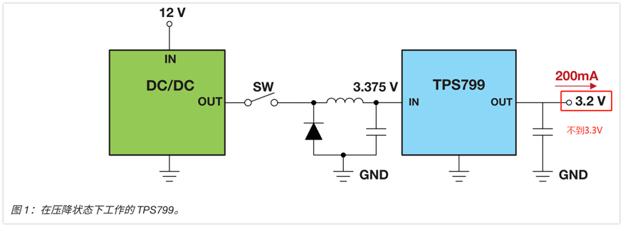
Although the output voltage should be regulated to 3.3V, the TPS799 does not have the headroom voltage required to maintain regulation. Therefore, the output voltage will start to follow the input voltage.
What factors determine pressure drop?
The voltage drop is mainly determined by the LDO architecture. To illustrate why, let's take a look at P-channel metal-oxide-semiconductor (PMOS) and N-channel MOS (NMOS) LDOs and compare their operation.
PMOS LDO
Figure 2 shows the PMOS LDO architecture. To regulate the desired output voltage, the feedback loop controls the drain-source resistance RDS. As VIN gradually approaches VOUT(nom), the error amplifier will drive the gate-source voltage VGS to increase negatively to reduce RDS and maintain regulation.
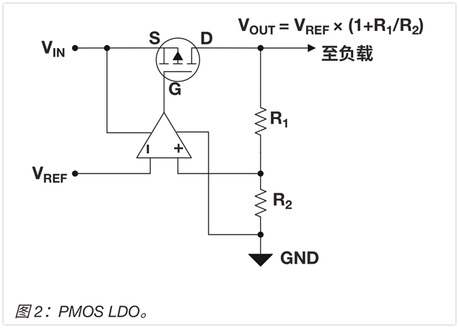
However, at a certain point, the error amplifier output will saturate at ground and will be unable to drive VGS further negative. RDS has reached its minimum value. Multiplying this RDS value by the output current IOUT will give you the dropout voltage.
Keep in mind that as VGS increases in the negative direction, the lower the RDS value that can be achieved. By increasing the input voltage, the VGS value can be increased in the negative direction. Therefore, PMOS architecture has lower voltage drop at higher output voltages. Figure 3 demonstrates this feature.
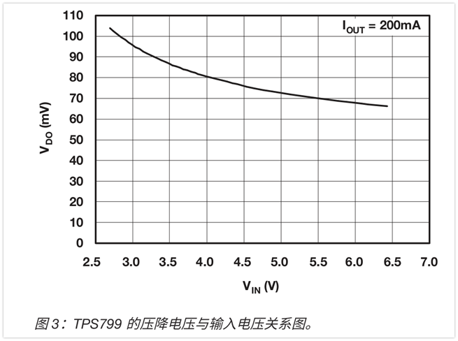
As shown in Figure 3, the dropout voltage of the TPS799 decreases as the input voltage (which also applies to the output voltage) increases. This is because VGS increases negatively as the input voltage increases.
NMOS LDO
The NMOS architecture is shown in Figure 4, and the feedback loop still controls RDS. However, as VIN approaches VOUT(nom), the error amplifier will increase VGS to reduce RDS, thus maintaining regulation.
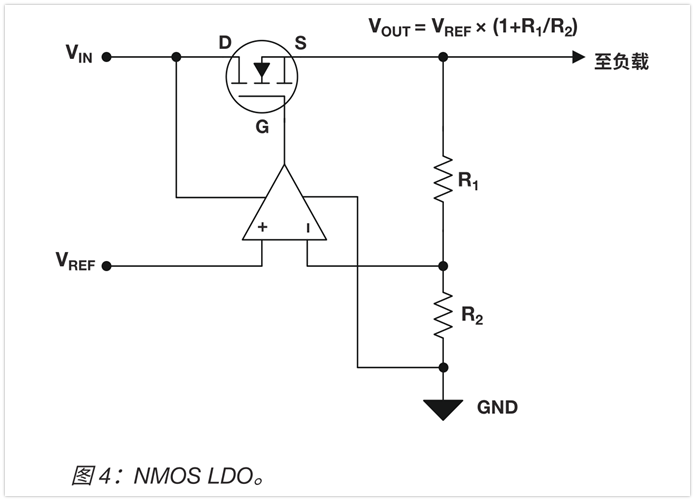
At a certain point, VGS cannot rise any higher because the error amplifier output will saturate at the supply voltage, VIN. When this state is reached, RDS is at its minimum value. Multiplying this value by the output current IOUT yields the dropout voltage.
This can cause problems, however, because the error amplifier output saturates at VIN and VGS decreases as VIN approaches VOUT(nom). This helps prevent ultra-low pressure drops.
Biased LDO
Many NMOS LDOs use an auxiliary voltage rail, the bias voltage VBIAS, as shown in Figure 5.
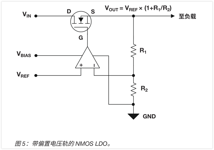
This voltage rail serves as the positive supply rail for the error amplifier and allows its output to swing all the way to VBIAS above VIN. This configuration allows the LDO to maintain a high VGS, resulting in ultra-low dropout at low output voltages. Sometimes an auxiliary voltage rail is not provided, but low dropout at a lower output voltage is still required. In this case, an internal charge pump can be used instead of VBIAS, as shown in Figure 6.
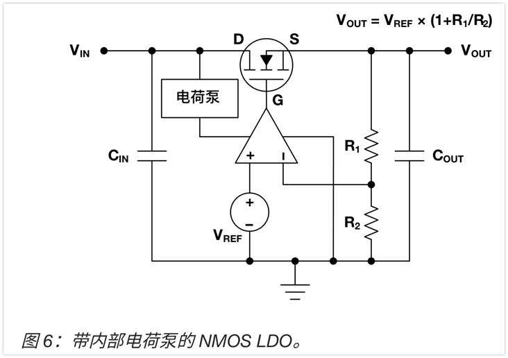
The charge pump will boost VIN so that the error amplifier can still generate a larger VGS value in the absence of the external VBIAS voltage rail.
other factors
In addition to architecture, voltage drop can be affected by several other factors, as shown in Table 1.
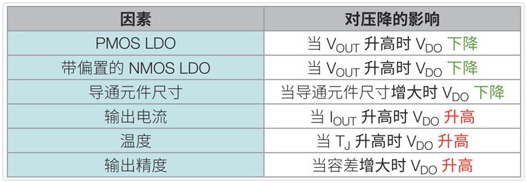
Obviously, the pressure drop is not a static value. While these factors can make LDO selection more complex, they can also help you select the most appropriate LDO based on your specific conditions.
 LDO capacitor selection

In order for the LDO to work properly, it needs an output capacitor. How to select the appropriate output capacitor is a common question when using LDOs for practical applications. So, let's explore the various things to consider when selecting an output capacitor and its impact on the LDO.
What is a capacitor
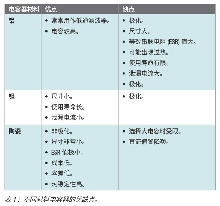
A capacitor is a device used to store electrical charge that contains one or more pairs of conductors separated by an insulator. Capacitors are typically made from materials such as aluminum, tantalum, or ceramic. Capacitors of various materials have their own advantages and disadvantages when used in systems, as shown in Table 1.
Ceramic capacitors are often ideal because they have minimal change in capacitance and are less expensive.
What is a capacitor?
A capacitor is a device used to store electric charge, while capacitance refers to the ability to store electric charge. Ideally, the value marked on a capacitor should be exactly the same as the capacitance it provides. But we are not in an ideal situation and cannot just look at the value marked on the capacitor. You will find out later that the capacitance of the capacitor may be only 10% of its rated value. This may be due to DC voltage bias derating, temperature change derating, or manufacturer tolerance.
DC voltage derating
Given the dynamic nature of capacitors (which store and dissipate charge in a non-linear manner), some polarization phenomena may occur without the application of an external electric field; this is known as "spontaneous polarization". Spontaneous polarization is caused by the material's inactive electric field, which provides the initial capacitance of the capacitor. Applying an external DC voltage to the capacitor generates an electric field that reverses the initial polarization and then "locks" or polarizes the remaining active dipoles into place. Polarization is related to the direction of the electric field within a dielectric.
As shown in Figure 1, a locked dipole does not react to AC voltage transients; therefore, the effective capacitance is lower than before the DC voltage was applied.
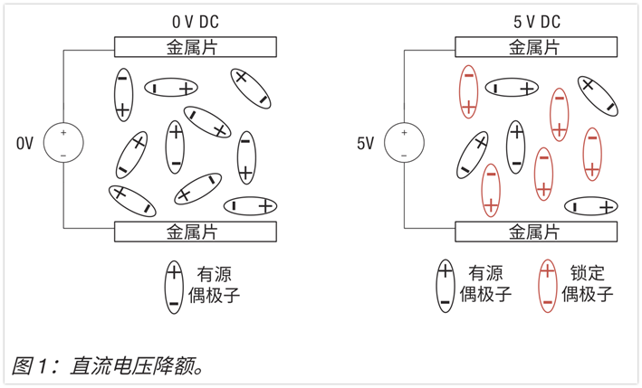
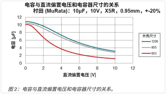
Figure 2 shows the effect of applying voltage to a capacitor and the resulting capacitance. Note that less capacitance is lost with larger case sizes; this is because the larger the case size, the more dielectric is present between the conductors, which reduces the electric field strength and reduces the number of locked dipoles.
Temperature derating
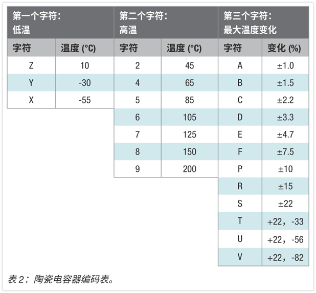
Like all electronic devices, capacitors are rated for temperatures higher than their rated performance. This temperature derating usually causes the capacitance of the capacitor to be lower than the value marked on the capacitor. Table 2 is the capacitor temperature coefficient rating decoding table.
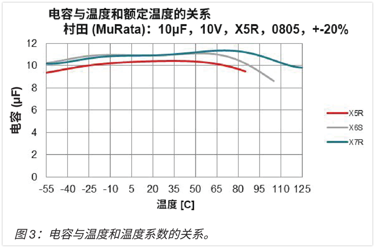
Most LDO junction temperatures typically range from -40°C to 125°C. Depending on this temperature range, X5R or X7R capacitors are ideal.
As shown in Figure 3, the effect of temperature on capacitance is much smaller than the effect of DC bias derating, which can reduce the capacitance value by 90%.
Practical application
常见的 LDO 应用可能是从 3.6V 电池获得输入电压,然后将其降低,为微控制器 (1.8V) 供电。在本例中,我们使用 10µF X7R 陶瓷电容器,0603 封装。0603 封装是指电容器的尺寸:0.06in x 0.03in。
我们来确定一下此应用中上述电容器的实际电容值:
a、直流偏置降额:从制造商提供的电容器直流偏置特性图表(图2)可以看出,直流偏置电压为 1.8V 时,电容值为 7µF。
b、温度降额:基于 X7R 编码,如果在 125°C 的环境温度下应用此电容器,电容值会另外下降 15%,此时的新电容值为 5.5µF。
c、 制造商容差:考虑到 ±20% 的制造商容差,最终的电容值为3.5µF。
可以看出,在上述条件下应用电容器时,10µF 电容器的实际电容值为 3.5µF。电容值已降低至标称值的 65% 左右。显然,上述所有条件并非对任何应用都适用,但务必要了解将电容器用于实际应用时电容值的范围。
尽管 LDO 和电容器乍看起来似乎很简单,但还有其他因素决定着 LDO 正常工作所需的有效电容。
 热性能
热性能

低压降稳压器 (LDO) 的特性是通过将多余的功率转化为热量来实现稳压,因此,该集成电路非常适合低功耗或 VIN 与 VOUT 之差较小的应用。考虑到这一点,选择采用适当封装的适当 LDO 对于最大程度地提高应用性能至关重要。这一点正是令设计人员感到棘手之处,因为最小的可用封装并不总能符合所需应用的要求。
选择 LDO 时要考虑的最重要特性之一是其热阻 (RθJA)。RθJA 呈现了 LDO 采用特定封装时的散热效率。RθJA 值越大,表示此封装的散热效率越低,而值越小,表示器件散热效率越高。
封装尺寸越小,RθJA 值通常越大。
例如,TPS732
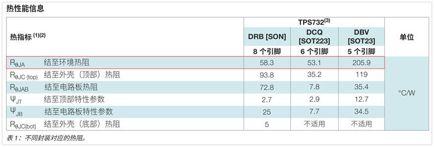
根据封装不同而具有不同的热阻值:小外形晶体管 (SOT)-23 (2.9mm x 1.6mm) 封装的热阻为205.9°C/W,而
SOT-223 (6.5mm x 3.5mm) 封装的热阻为 53.1°C/W。这意味着 TPS732 每消耗1W 功率,温度就会升高205.9°C 或 53.1°C。这些值可参见器件数据表的“热性能信息”部分,如表 1 所示。
是否选择了适合的封装?
建议的 LDO 工作结温介于-40°C 至 125°C 之间;同样,可以在器件数据表中查看这些值,如表 2 所示。

这些建议的温度表示器件将按数据表中“电气特性”表所述工作。可以使用公式 1 确定哪种封装将在适当的温度下工作。

其中 TJ 为结温,TA 为环境温度,RθJA 为热阻(取自数据表),PD 为功耗,Iground 为接地电流(取自数据表)。
下面给出了一个简单示例,使用 TPS732 将 5.5V 电压下调至3V,输出电流为 250mA,采用 SOT-23 和 SOT-223 两种封装。

热关断
结温为 154.72°C 的器件不仅超过了建议的温度规范,还非常接近热关断温度。关断温度通常为 160°C;这意味着器件结温高于 160°C 时会激活器件内部的热保护电路。此热保护电路会禁用输出电路,使器件温度下降,防止器件因过热而受到损坏。
当器件的结温降至 140°C 左右时,会禁用热保护电路并重新启用输出电路。如果不降低环境温度和/或功耗,器件可能会在热保护电路的作用下反复接通和断开。如果不降低环境温度和/或功耗,则必须更改设计才能获得适当的性能。
一种比较明确的设计解决方案是采用更大尺寸的封装,因为器件需要在建议的温度下工作。下文介绍了有助于最大程度地减少热量的一些提示和技巧。
增大接地层、VIN 和 VOUT 接触层的尺寸
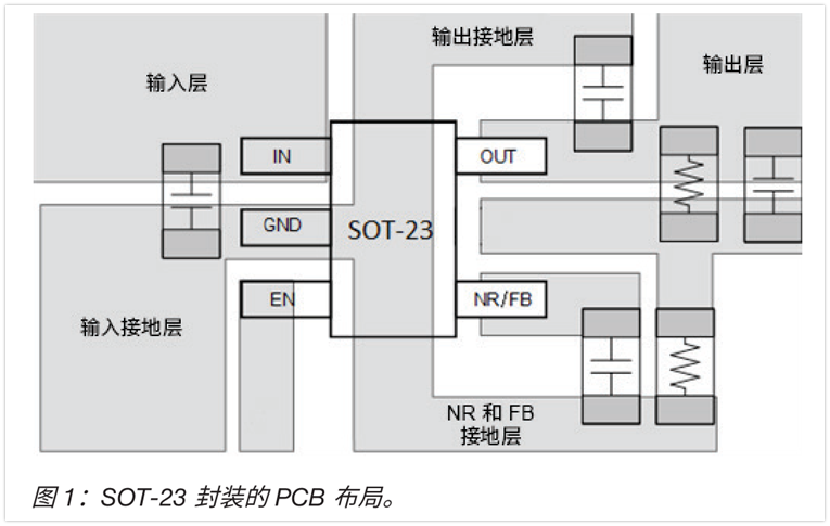
当功率耗散时,热量通过散热焊盘从 LDO 散出;因此,增大印刷电路板 (PCB) 中输入层、输出层和接地层的尺寸将会降低热阻。
如图 1 所示,接地层通常尽可能大,覆盖 PCB 上未被其他电路迹线占用的大部分区域。该尺寸设计原则是由于许多元件都会生成返回电流,并且需要确保这些元件具有相同的基准电压。最后,接触层有助于避免可能会损害系统的压降。大的接触层还有助于提高散热能力并最大限度地降低迹线电阻。增大铜迹线尺寸和扩大散热界面可显著提高传导冷却效率。
在设计多层 PCB 时,采用单独的电路板层(包含覆盖整个电路板的接地层)通常是个不错的做法。这有助于将任何元件接地而不需要额外连线。元件引脚通过电路板上的孔直接连接到包含接地平面的电路板层。
串联电阻 分担功耗
可以在输入电压侧串联电阻,以便分担一些功耗;图 3 所示为相关示例。该技术的目标是使用电阻将输入电压降至可能的最低水平。
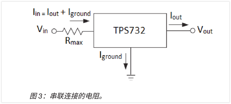
由于 LDO 需要处于饱和状态以进行适当调节,可以通过将所需的输出电压和压降相加来获得最低输入电压。公式 2 表示了LDO 的这两种属性的计算方式:

使用 TPS732 示例中的条件(输出 250mA 电流,将 5.5V 调节至 3V),可以使用公式 3 计算电阻的最大值以及该电阻消耗的最大功率:

选择适合的电阻,确保不会超过其“额定功耗”。此额定值表示在不损坏自身的情况下电阻可以将多少瓦功率转化为热量。因此,如果 VIN = 5.5V、VOUT = 3V、VDROPOUT = 0.15V(取自数据表)、IOUT = 250mA 且 IGROUND = 0.95mA(取自数据表),则:

 电流限制
电流限制

在一些外部条件和情况下,LDO 可能会出现意外的高流耗。如果此高电流传输到其他正被供电的电子系统,会对大多数电子系统以及主机电源管理电路造成损害。选择具有电流限制和内部短路保护的 LDO,将有助于防止产生这种不良影响,并在设计整体电源管理模块时提供额外保护。
什么是电流限制功能,该功能如何运作?
LDO 中的电流限制定义为,建立所施加电流的上限。与恒流源不同,LDO 按需输出电流,同时还会控制调节的总功率。
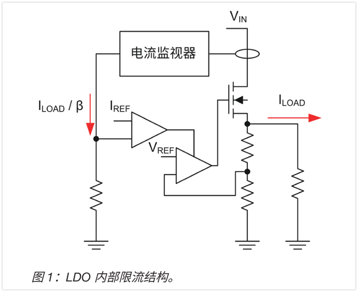
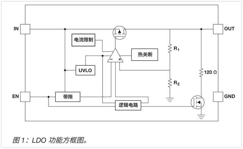
Current limiting is achieved through internal circuitry that controls the output stage transistors within the LDO, see Figure 1. This is a typical LDO current limiting circuit, often referred to as "brick wall" current limiting because the circuit suddenly stops outputting current when the limit is reached. In this internal circuit, the LDO measures the feedback output voltage and simultaneously measures the scaled image of the output current relative to an internal reference (IREF).
Brick wall current limit
In brickwall current limiting, an upper current limit is defined and the LDO gradually increases the supply current until the current limit is reached. Once the current limit is exceeded, the output voltage is no longer regulated and is determined by the load circuit resistance (RLOAD) and the output current limit (ILIMIT) (Equation 1):

As long as the junction temperature is within an acceptable range (TJ < 125°C) and the thermal resistance (θJA) allows normal power dissipation, the pass transistor continues this operation and dissipates power. When VOUT is too low and reaches the upper temperature limit, the thermal shutdown function will disconnect the device to protect it from permanent damage. After the device cools down, it will turn back on and regulation can continue. This is particularly important in the event of a possible short circuit, as the LDO will continue to regulate VOUT to 0V.
For example, TI's TPS7A16 can limit high current output over a wide voltage range. Figure 2 shows an example of the behavior of the current limit feature at 30V input conditions. It can be seen that once the current limit is exceeded, the LDO continues to output current at the limit but no longer regulates VOUT to 3.3V. Once the 105mA thermal limit is exceeded, the thermal shutdown feature is initiated.
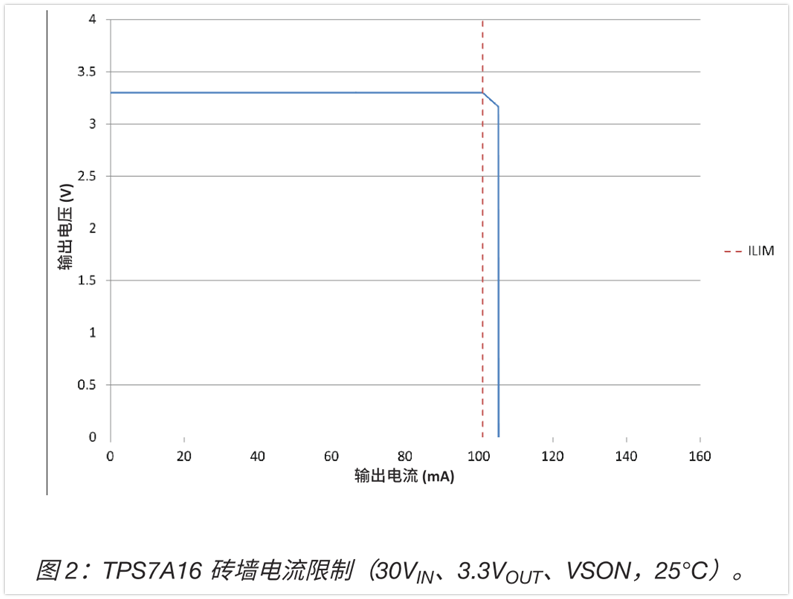
This current-limiting feature facilitates charging of NiCd and NiMH single-cell batteries, since both types of batteries require a constant supply of current. The battery voltage changes as the battery charges, and an LDO such as the TPS7A16 helps maintain a constant current within a limit (I).
Prevent reverse current
In most low-dropout regulators (LDOs), current flows in a specific direction, and current flowing in the wrong direction can create major problems! Reverse current is the current flowing from VOUT to VIN rather than from VIN to VOUT. This current typically passes through the LDO's body diode rather than through the normal conductive path, potentially causing long-term reliability issues or even damaging the device.
An LDO has three main components (see Figure 1): a bandgap reference, an error amplifier, and a pass-on field-effect transistor (FET). In a typical application, a pass-on FET conducts current between source and drain like any standard FET. The doped region used to create the body of the FET, called the bulk, is connected to the source; this reduces the amount of threshold voltage variation.
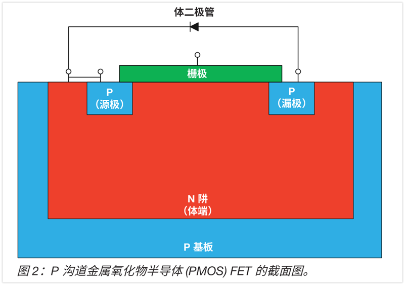
Connecting the bulk to the source has the disadvantage of creating a parasitic body diode in the FET, as shown in Figure 2. This parasitic diode is called the body diode. In this configuration, the body diode will conduct when the output exceeds the input voltage plus the VFB of the parasitic diode. Reverse current flowing through this diode may cause device damage by causing temperature rise, electromigration, or latch-up effects.
When designing an LDO, it is important to take reverse current and how to prevent it into consideration. There are four methods to prevent reverse current flow: two are implemented at the application level and two are implemented during the integrated circuit (IC) design process.
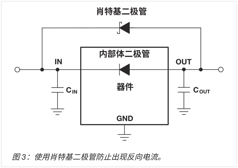
Use Schottky diodes
As shown in Figure 3, using a Schottky diode between the output and input prevents the body diode in the LDO from conducting when the output voltage exceeds the input voltage. You have to use Schottky diodes, Schottky diodes have lower forward voltage whereas conventional diodes have much higher forward voltage compared to Schottky diodes. In normal operation, the Schottky diode is reverse biased and does not carry any current. Another advantage of this approach is that the dropout voltage of the LDO does not increase when a Schottky diode is placed between the output and input.
Use diode before LDO
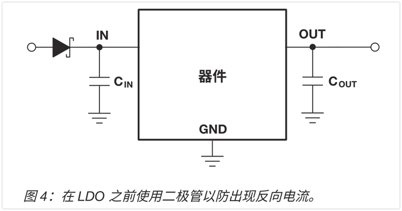
As shown in Figure 4, this method uses a diode before the LDO to prevent current from flowing back to the supply. This is an effective way to prevent reverse current flow, but it also increases the necessary input voltage required to prevent voltage drop across the LDO. The diode placed at the input of the LDO becomes reverse biased during reverse current conditions and does not allow any current to flow. This method is similar to the next method.
Add an additional FET
LDOs designed to prevent reverse current flow usually have an additional FET added to help prevent reverse current flow. As shown in Figure 5, the source stages of the two FETs are placed back-to-back so that the body diodes are facing each other. Now, when a reverse current condition is detected, one of the transistors will open and current will not be able to flow through the diodes placed back to back.
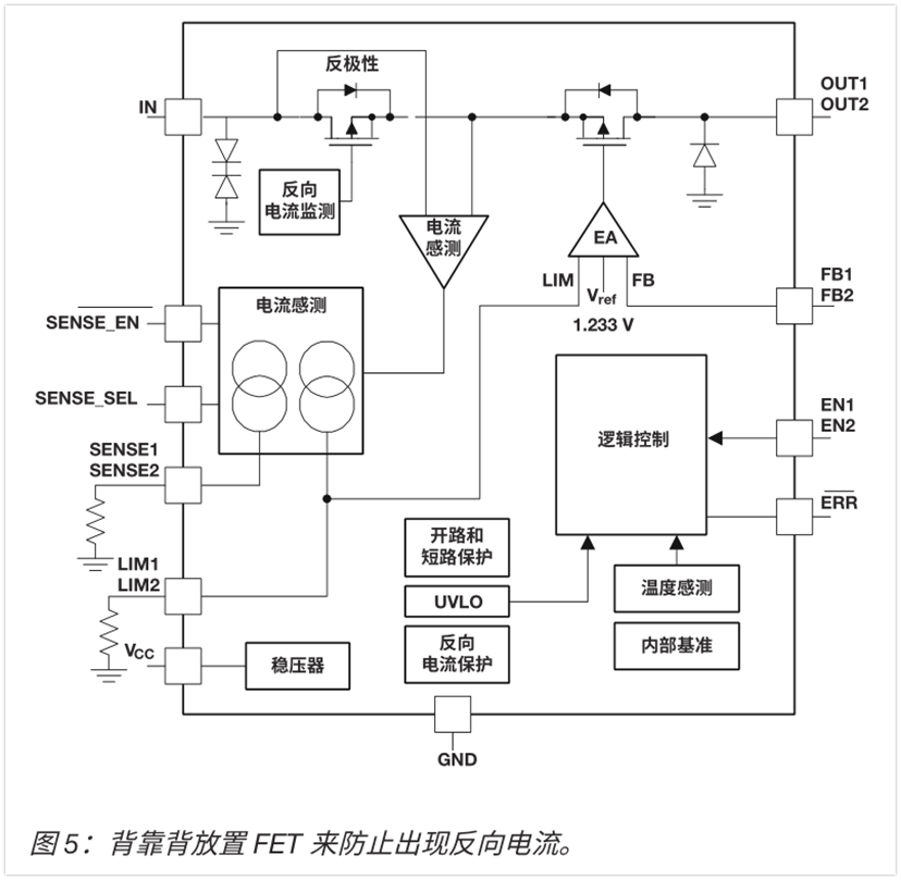
One of the biggest disadvantages of this approach is that the dropout voltage essentially doubles when using this architecture. To reduce the dropout voltage, the size of the metal-oxide-semiconductor field-effect transistor (MOSFET) needs to be increased, thus increasing the overall solution size. LDOs used in automotive applications, such as TI's TPS7B7702-Q1, use this method to prevent reverse current flow.
 power supply rejection ratio

One of the most popular advantages of low-dropout regulators (LDOs) is their ability to attenuate the voltage ripple generated by switch-mode power supplies. This is particularly important for signal conditioning devices such as data converters, phase-locked loops (PLLs), and clocks, where noisy supply voltages can affect the performance of such devices. Power Supply Rejection Ratio (PSRR) is still often mistaken as a single static value. Let’s discuss what PSRR is and what factors affect it.
What is PSRR?
PSRR is a common specification listed in many LDO data sheets. It specifies the degree to which AC components of a specific frequency are attenuated from the LDO input to the output. Equation 1 expresses PSRR as:

Equation 1 shows that the higher the attenuation, the greater the PSRR value in decibels will be. (Some vendors use a negative sign to indicate attenuation, while most, including TI, do not.)
PSRR specified at 120Hz or 1kHz can often be found in the electrical characteristics table of the datasheet. However, using this parameter alone may not determine whether a given LDO meets specific filtering requirements. The reasons are explained in detail below.
PSRR that does fit the application
Figure 1 shows a DC/DC converter that regulates a 12V rail to 4.3V. The TPS717 is connected behind, which is an LDO with a high PSRR value and is used to regulate the 3.3V voltage rail. The ripple generated by switching on the 4.3V rail is ±50mV. The LDO's PSRR will determine the amount of ripple remaining at the output of the TPS717.

To determine the degree of attenuation, you must first know the frequency at which ripple occurs. Assume that the corresponding frequency in this example is 1MHz since this value is right in the middle of the common switching frequency range. As you can see, specifying PSRR values at 120Hz or 1kHz does not help this analysis. Instead, you must refer to the PSRR graph in Figure 2.
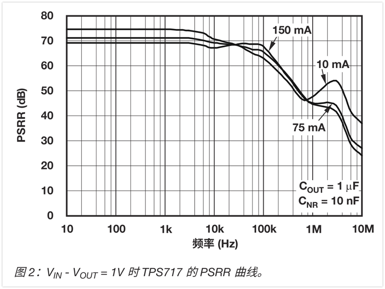
PSRR is specified as 45dB at 1MHz under the following conditions.
IOUT = 150mA
VIN - VOUT = 1V
COUT = 1μF
It is assumed that these conditions correspond to the specific application conditions. In this case, 45dB is equivalent to an attenuation factor of 178. It can be expected that a ±50mV ripple at the input will be reduced to ±281µV at the output.
Change conditions
However, let's say you change the conditions and decide to reduce VIN - VOUT to 250mV in order to regulate more efficiently. Then you need to refer to the curve in Figure 3.
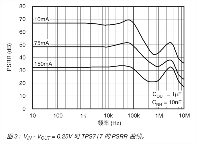
It can be seen that if all other conditions are kept constant, the PSRR at 1MHz is reduced to 23dB, which is an attenuation factor of 14. This is because the complementary metal oxide semiconductor (CMOS) pass element enters the triode (or linear) region, that is, as the value of VIN -VOUT approaches the dropout voltage, PSRR begins to decrease. (Remember, dropout voltage is a function of output current and other factors. Therefore, lower output current reduces dropout voltage, helping to improve PSRR.)
Changing the capacitance value of the output capacitor also has an effect, as shown in Figure 4.
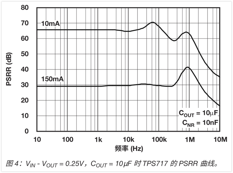
When increasing the value of the output capacitor from 1µF to 10µF, the PSRR at 1MHz increases to 42dB, although the value of VIN - VOUT is still 250mV. The high-frequency peaks in the curve have been shifted to the left. This is due to the impedance characteristics of the output capacitor. By appropriately adjusting the output capacitor value, the degree of attenuation can be adjusted or increased to be consistent with a specific switching noise frequency.
Adjust all parameters
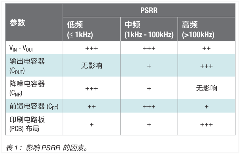
The PSRR of a specific application can be improved simply by adjusting VIN - VOUT and the output capacitance. But the factors that affect PSRR are not limited to these two items. Table 1 outlines several factors that influence this.
references
· END ·


 京公网安备 11010802033920号