Article count:10827 Read by:13690842

Featured Content
Account Entry

Understanding the three levels of circuit integration in one article

Latest update time:2022-04-18
    Reads:

Levels of Integration

The integration of electronic systems is mainly divided into three levels: on-chip integration, in-package integration, and PCB board-level integration, as shown in the following figure:
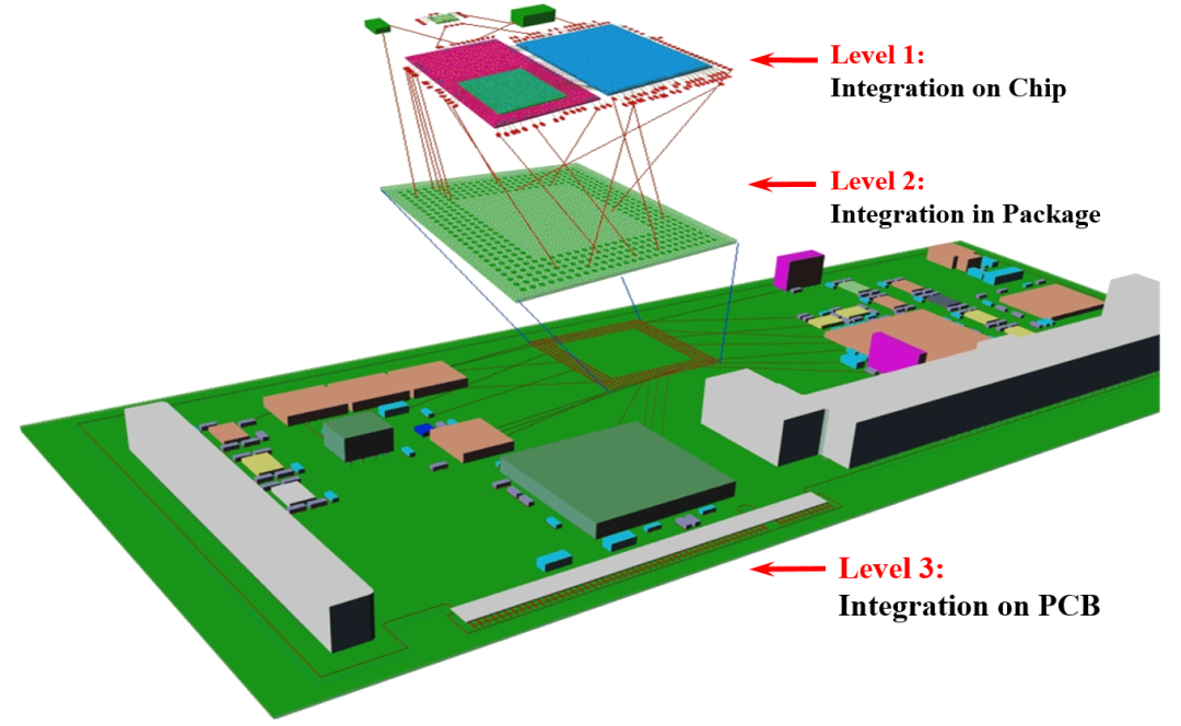

The basic unit integrated on the chip is the transistor, which we call a functional cell. A large number of functional cells are integrated together to form a chip.

The basic unit integrated in the package is the bare chip or chiplet completed in the previous step, which we call the functional unit (Function Unit). These functional units are integrated in the package to form SiP.

The basic unit integrated on the PCB is the package or SiP completed in the previous step, which we call a microsystem. These microsystems are integrated on the PCB into a larger system.

It can be seen that the levels of integration are carried out step by step. The functions of each level of integration are constantly improved on the basis of the previous level, and the scale is constantly expanded.

At the PCB level, the functions of the electronic system have become relatively complete, and the scale has been enlarged to a level suitable for human control. Together with other components, it constitutes the system that people use most often - the common system, such as the mobile phones or computers we use every day.

On-chip integration

The transistor on a chip is called a functional cell because it is the smallest functional unit that cannot be divided.

The number of functional cells has also become an important indicator of the advancement of the system. The number of cells in the human body is 40 to 60 trillion. If the system wants to become a truly intelligent system like a human, the number of functional cells it contains may also reach the same level.

In order to integrate more functional cells , transistors can only be made smaller and smaller. The size of transistors today may be only one billionth of the size of the original transistors when they were first invented , but their basic functions have not changed.

To integrate on a chip, we must first create functional cells and integrate them together. How are these transistors, which serve as functional cells, created and integrated together? From a very simple perspective, we need to understand three types of materials and three types of processes.

Conductors, semiconductors, insulators

Although there are many materials on the chip, the materials used in modern integrated circuits almost exhaust the periodic table. All materials can be divided into three categories: conductors, semiconductors, and insulators.

Conductors are responsible for transmitting electrons, and insulators are responsible for isolating electrons. The most important of these is naturally semiconductors, because they are variable. Sometimes they become conductors (on), allowing electrons to pass through, and sometimes they become insulators (off), blocking electrons from passing through. Moreover, this change is controllable by designing a special structure and applying current or voltage.

In conductors, the conduction band overlaps with the valence band, and there is no band gap, so electrons can easily move and form a current under an external electric field; in semiconductors, a small number of electrons can jump to the conduction band and form a current under an external electric field; in insulators, electrons cannot cross the band gap and therefore cannot form a current.

Additive process, subtractive process, graphic transfer
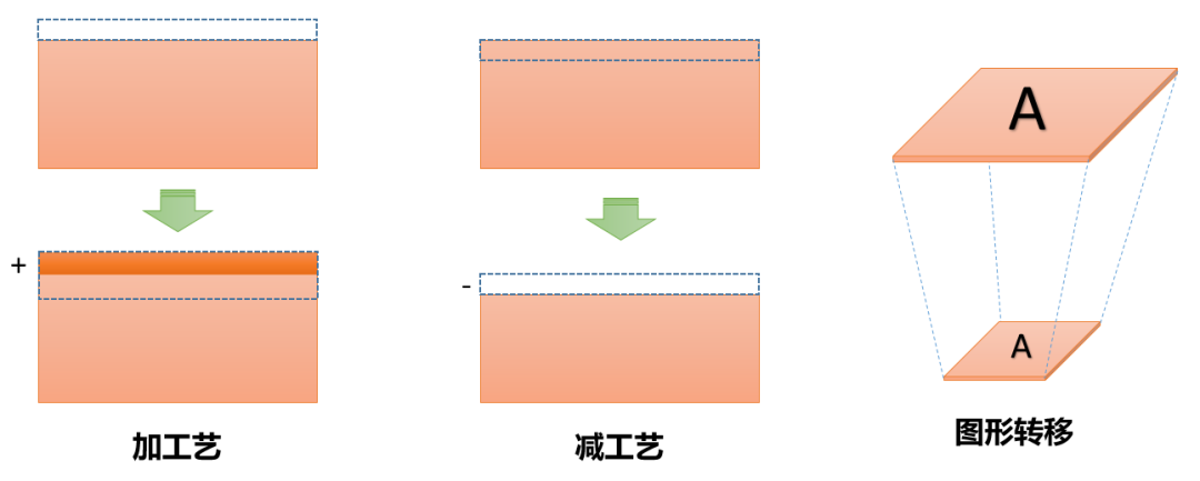
There are many processes for manufacturing chips, and there are thousands of process flows to complete the manufacturing of a chip. These processes can be divided into three categories: additive process, subtractive process , and pattern transfer.
Additive process Simply put, it is to add materials to the substrate. For example, ion implantation, sputtering, chemical vapor deposition CVD, physical vapor deposition PVD, etc. can all be classified as additive processes.
Subtractive process Simply put, it is the removal of materials , such as etching, chemical mechanical polishing CMP, wafer leveling, etc. can be classified as subtractive process .
Pattern transfer is the most common and most difficult of the three types of processes , because each step of the additive or subtractive process is basically based on pattern transfer. Pattern transfer is to transfer the designed pattern to the wafer, which involves masks, photolithography, and photoresist.
The transfer of graphics is actually the transfer of human thinking and wisdom .
Pattern transfer is required before and after each step of the additive or subtractive process so that a specific pattern can be made on the chip.
These graphics are superimposed in multiple layers, combining semiconductors, conductors, and insulators to form a specific three-dimensional structure, creating functional cells on the wafer plane and realizing corresponding functions.
Three types of materials + three types of processes can create such a complex chip, which really proves what the ancients said: "One gives birth to two, two gives birth to three, and three gives birth to all things."
After thousands of processes, the product integrated on the chip is a wafer. After the wafer is cut, it forms a chip or chiplet, preparing for the next level of integration.

Integration in package

Not all chips or core particles need to be integrated in the package. Single chips can also be directly packaged and applied on PCB boards. However, as Moore's Law becomes increasingly ineffective, in-package integration is gaining more and more attention. Concepts such as SiP, advanced packaging, chiplet, heterogeneous integration, 2.5D, and 3D are becoming the focus of the industry, and in-package integration has finally ushered in its spring.

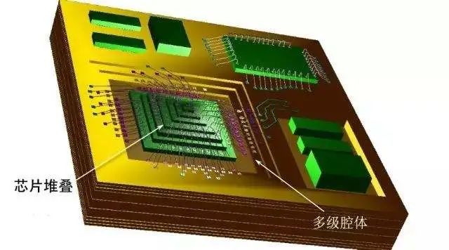
In-package integration does not utilize the properties of semiconductors, so the materials used for in-package integration are mainly divided into two categories: conductors and insulators. The main purpose of integration is to integrate the chips or core particles completed at the previous level (integration on the chip) in the package and electrically interconnect them to form a microsystem.
The initial packaging was single-chip and there was no concept of integration. The main functions of traditional single-chip packaging are three: chip protection, scale enlargement, and electrical connection .
Multi-chip packaging represented by SiP adds three functions based on traditional packaging: improving functional density, shortening interconnection length, and performing system reconstruction .
Integration within the package relieves the pressure of on-chip integration and is thus seen as a powerful weapon to delay the end of Moore's Law.
Since the integration within the package does not require the manufacture of functional cells (Transistor), but only requires the assembly of functional units (chiplets), its integration difficulty is much lower than that on the chip.
Another feature of in-package integration is its high flexibility, which can be divided into five integration dimensions: 2D, 2D+, 2.5D, 3D, and 4D .
The result of in-package integration is the formation of functional units represented by SiP and advanced packaging, which we can call microsystems.

Integration on PCB

In terms of the history of electronic integration, integration on PCB should be the earliest to appear. PCB appeared 11 years earlier than packaging and 22 years earlier than integrated circuits.

Before the advent of PCBs, components were directly connected with wires, which was not only very messy but also difficult to improve integration density.

Although PCB has the earliest history compared with integrated circuits and packages, the development of integrated technology on PCB is relatively slow due to the constraints of package size and package pin density. From the initial single-sided board to double-sided board and multi-layer board, the assembly process has also developed from plug-in type to surface mount SMT, and the assembly density is getting higher and higher.

Today, components are basically installed on double-sided PCBs, and the number of board layers can reach dozens. High-density HDI boards, rigid-flexible boards, microwave circuit boards, embedded device boards, etc. are widely used.

Like the integration within the package, the integration on the PCB does not use the characteristics of semiconductors, so the materials used are mainly divided into two categories: conductors and insulators. The main purpose of integration is to integrate the microsystem modules completed at the previous level (integration within the package) again and interconnect them electrically, and together with other components, form a normal system, such as our commonly used mobile phones and computers.


Integrated links

We have described the three levels of integration of electronic systems above: on-chip integration, in-package integration, and PCB board-level integration. Each level of integration is divided into different links.

Integrated links on chip

The integration on the chip is mainly divided into two major links: device manufacturing and metal interconnection, also known as the front-end process FEOL and the back-end process BEOL.
  • Device manufacturing (front-end process)
Device manufacturing is to manufacture transistors, resistors, capacitors, diodes, etc. , which we call functional cells , on single-crystal silicon wafers through photolithography, etching, ion implantation, sputtering, chemical vapor deposition, physical vapor deposition , chemical mechanical polishing , wafer leveling and other process steps. The current 5nm process can manufacture more than 100 million transistors on an area of ​​1mm².
The manufacturing process of transistors mainly includes isolation, gate structure, source and drain, contact hole formation processes, which are generally referred to as front-end process (FEOL, Front End of Line).
Single crystal silicon can be formed into semiconductors with different doping concentrations such as N, N+, N-, P, P+, P-, etc. through ion implantation, while polycrystalline silicon is used as gate or resistor.
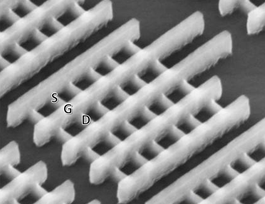
The figure below shows a photograph of a FinFET transistor under a microscope, in which the taller white beam is the gate G, the shorter beam is the Fin, whose width is about 0.67 times the width of the gate, and the source S and drain D are on both sides of the gate.
  • Metal interconnection (back-end process)

After the transistor layer is manufactured, contact holes are made through metals such as tungsten to connect the transistor and the first layer of wiring, and then electrical interconnection is carried out through multi-layer metal wiring and vias. Early chips used aluminum wiring, and now chips mostly use copper wiring.

The manufacture of multi-layer metal wiring used to connect devices such as transistors mainly includes the deposition of dielectrics between interconnect lines, the formation of metal lines, and the formation of lead pads, which is generally called the back-end of line (BEOL).

The conductors used in metal interconnects include metals such as tungsten, copper, and aluminum, while the insulators include silicon oxide, silicon nitride, high dielectric constant films, low dielectric constant films, polyimide, and the like.

The figure below shows a photo of the metal interconnect lines on the chip under a microscope. It can be seen that there are multi-layer wiring structures. The current process can support more than 10 layers of metal wiring.

The more advanced the integrated circuit technology is, the smaller the structure size is, and various effects emerge one after another. In order to solve these effects and produce functioning transistors, more and more types of elements are used, which is almost a movement to exhaust the periodic table.

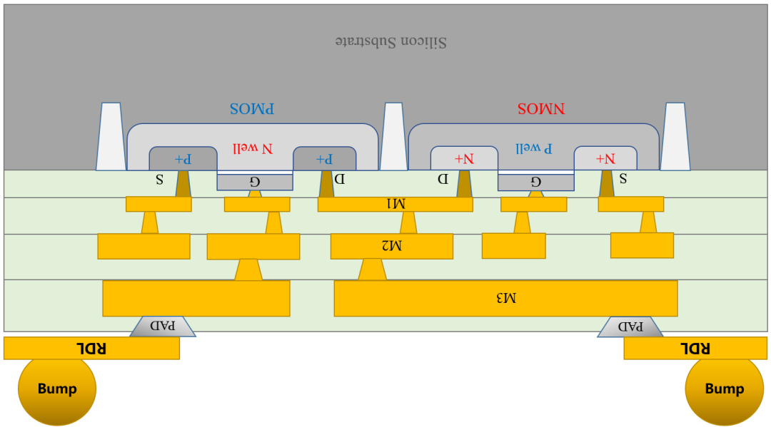
The figure below shows the schematic diagram of the structure of the front-end process FEOL and the back-end process BEOL. Transistors are first manufactured on a silicon substrate, and then they are connected through metal interconnects and led out to the chip's PAD.

Integrated links in the package

The early packaging was relatively simple, mainly playing the role of chip protection, scale enlargement, and electrical interconnection. Its schematic diagram is roughly as follows: the chip PAD is connected to the package substrate or lead frame through the bonding wire, and then connected to the external pins. According to the arrangement of the pins, it can be divided into BGA, CGA, QFP, LCC, SOP, DIP and other packaging forms.

Traditional packaging has a relatively simple internal structure, which uses bonding wires to connect the chip pins to the lead frame or substrate, while the external pin arrangement is diverse. Therefore, when people talk about packaging, they are most interested in its various external packaging forms. Therefore, we say: traditional packaging focuses on the outside rather than the inside.
In the era of SiP and advanced packaging, this situation has changed dramatically. The external packaging forms of SiP and advanced packaging have gradually been unified into BGA, CGA and other packaging forms with more pins and higher interconnection density. However, due to the integrated functions inside the package, its structure has become more and more complex. People's attention to packaging has gradually shifted from external packaging forms to internal packaging structures. Therefore, we say: Advanced packaging focuses on the inside rather than the outside .
In order to improve the functional density within the package, it is necessary to integrate more functional units within the package. The traditional bonding wire connection method can no longer meet the requirements. People have invented a variety of advanced packaging technologies. Let's take a look at the most typical technologies.
  • RDL and TSV fabrication on chip
The wiring is done on the chip surface, and the PAD is connected to a more spacious position through the RDL (Redistribution Layer) redistribution layer to create a bump, which we call an extension of the XY plane.
Then through the Bump, the chip can be directly installed on the substrate. This process is called flip chip. Look at the picture below and you will understand why it is called flip chip.
The flip-chip process appeared in the 1960s and is basically a contemporary product of the bonding wire. It has a long history and I generally do not call it advanced packaging.
Since flip-chip chips cannot be stacked, they cannot be extended in the Z-axis. Therefore, people invented a through-hole technology that can penetrate the entire chip body, which is called TSV (Through Silicon Via) technology.
TSV has many process difficulties to overcome. I think the most important ones to be solved are TSV location selection and aperture reduction.
Because TSV needs to pass through the entire chip body, the internal circuit connection and transistors will be damaged if the location is not chosen properly, so the location selection is very important. The reduction of the aperture is also to occupy as little space on the chip as possible. After all, 1mm² area can accommodate more than 100 million transistors, and if it is not done properly, hundreds of millions of transistors will be lost in an instant.

However, the current TSV technology is becoming increasingly powerful. It is said that up to one million TSVs can be etched in an area of ​​1mm², which can fully meet the needs of high-density interconnection.

The figure below is a schematic diagram of TSV on the chip. Through TSV, the upper and lower surfaces of the chip can be connected through metal conductors, preparing for chip stacking.

It is extremely difficult to make TSV on a chip, and only leading foundries can do it. This type of TSV is usually called 3D TSV.

In order to further improve the integration level, people have invented a method of making TSV on a silicon substrate interposer, which is called 2.5D TSV.

  • RDL and TSV fabrication on Interposer

Interposer is called silicon transfer board, interposer, which can provide higher interconnection density than ordinary substrate.

The following figure shows a typical silicon adapter board , with 3 metal layers on the top and 2 metal layers on the bottom, connected by silicon vias in the middle. We call it a 3+2 structure.

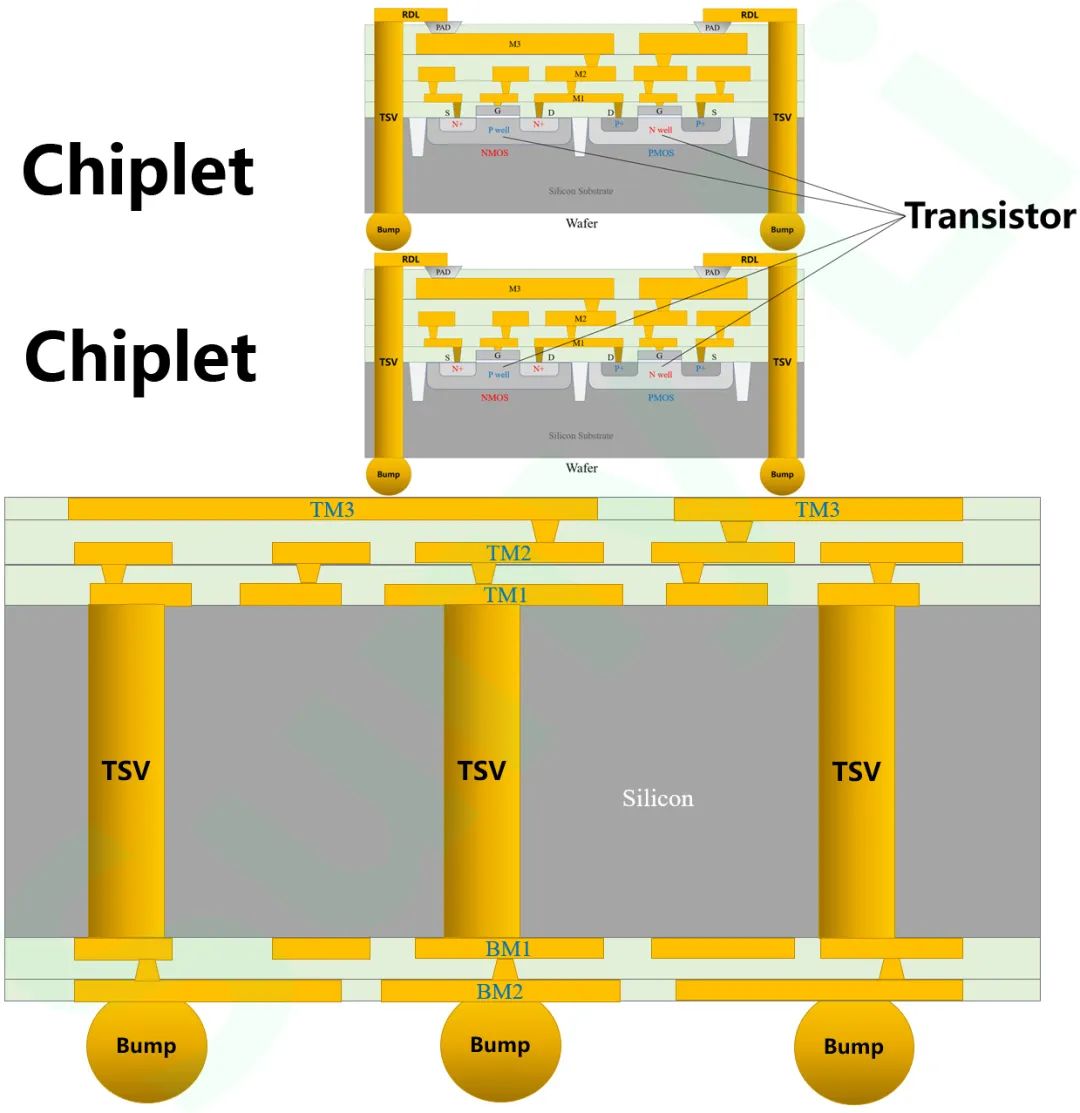
The TSV on the interposer is usually larger in size and smaller in density than the TSV on the chip, and is also easier to manufacture. Currently, this type of 2.5D TSV can be processed by OSAT packaging and testing factories.
After making the Interposer, we can install the chip or core on the silicon adapter board.
As shown in the figure below, because the structure includes 3D TSV and 2.5D TSV, we call it 2.5D+3D advanced packaging.


  • Interconnection fabrication on Substrate

Next, we need to make the packaging substrate. There are many types of packaging substrate materials, which can be divided into organic substrates and ceramic substrates.

Organic substrates are made of organic resin and glass fiber cloth as the main materials, and the conductor is usually copper foil. Organic resins usually include: epoxy resin (FR4), BT resin (bismaleimide triazine resin), PPE resin (polyphenylene ether resin), PI resin (polyimide resin), etc.
Ceramic substrates have better mechanical and thermal properties than organic substrates, and usually include HTCC , LTCC , aluminum nitride and other ceramic substrates.
The figure below shows a typical organic substrate structure. The middle 4 layers are made by the Laminate lamination method, and the 2 layers on the upper and lower surfaces are made by the Buildup lamination method. We call it a 2+4+2 structure.

The package substrate generally has components mounted on the top and is connected to the PCB through BGA on the bottom.
  • Device assembly and packaging

Next, we assemble the Chiplet, Inteposer, and Substrate and process them using advanced packaging technology to form a complete advanced package.

The result of integration within the package has the functions of the system and is small in size. We can call it SiP or microsystem.

Integrated links on PCB

After the chip is integrated in the package, its size is not large enough. In addition, some discrete components, such as large capacitors and transformers, cannot be integrated into the chip package. Therefore, PCB is always indispensable for electronic products.
  • Fabrication of PCB interconnection lines
The manufacturing process of PCB is similar to that of organic substrate. Its wiring density is not as high as that of organic substrate and its structure is relatively simple.
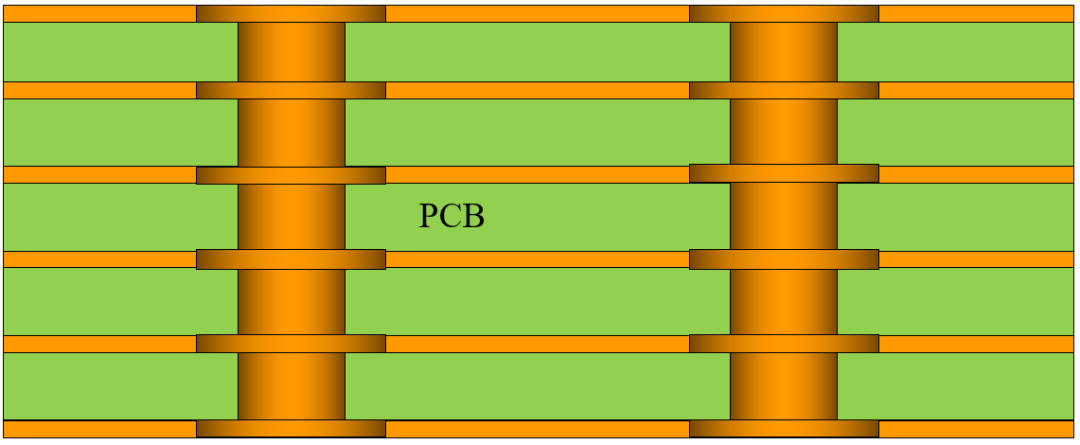
Through-hole structures are mostly used on PCBs. Although high-density HDI boards now also use blind and buried hole structures, through-holes have been widely used in PCBs due to their simple structure and low cost.
The figure below shows a 6-layer through-hole structure PCB, through which the devices can be fixed and electrically interconnected.
  • Component assembly on PCB
After the PCB is processed, the packaged components need to be assembled on the PCB, as shown in the figure below, and connected to external connectors and external devices through the PCB.


Full picture from transistor to PCB

Below, we give a full picture of the integration from transistor to PCB, as shown below:


(Readers are advised to save this picture, because this picture may be the first in the industry to show the 5-level circuit integration from transistor to PCB , drawn by hand by Suny Li. Because it is a schematic diagram, it is not drawn strictly according to the scale. In fact, the size is enlarged by about 1,000,000 times from transistor to PCB)

After the transistor (NMOS or PMOS) is manufactured on the silicon substrate, it is connected to the metal wiring on the chip through contact holes, then to the chip's pad, then to 3D TSV through RDL, connected to the RDL and 2.5D TSV on the silicon adapter board through uBump, then connected to the package substrate through Bump, and then connected to BGA through the wires and vias on the package substrate, and finally to the wiring and vias on the PCB.
From transistor to PCB, the complete 5-level electrical signal path is as follows:
Transitor→Contact→Copper→Pad RDL¹→3DTSV→uBump RDL²→2.5DTSV→Bump Trace¹→Via¹→BGA Trace²→Via²→PCB
On integrated circuit chips, humans have achieved the creation of functions through transistors, reconstructed functions and enlarged scale on SiP or advanced packaging , and further reconstructed functions and enlarged scale on PCBs .
From transistors to PCBs, the scale is magnified a million times to match the scale of humans themselves.
Finally, PCB and other components are organically combined together to become the mobile phones that modern people can operate anytime and anywhere and the computers that they can hardly leave at work.

Add WeChat and reply " join group"

Invite you to join the technical exchange group!

Domestic chips|Automotive electronics|Internet of Things|New energy|Power supply|Industry|Embedded...

Reply to any content you want to search in the official , such as problem keywords, technical terms, bug codes, etc., and you can easily get relevant professional technical content feedback . Go and try it!


If you want to see our articles more often, you can go to our homepage, click the "three dots" in the upper right corner of the screen, and click "Set as Star".

Welcome to scan the QR code to follow us


Latest articles about

 
EEWorld WeChat Subscription

 
EEWorld WeChat Service Number

 
AutoDevelopers

About Us Customer Service Contact Information Datasheet Sitemap LatestNews

Room 1530, Zhongguancun MOOC Times Building,Block B, 18 Zhongguancun Street, Haidian District,Beijing, China Tel:(010)82350740 Postcode:100190

Copyright © 2005-2024 EEWORLD.com.cn, Inc. All rights reserved 京ICP证060456号 京ICP备10001474号-1 电信业务审批[2006]字第258号函 京公网安备 11010802033920号