Home >
Basic Circuits >Digital Circuits > Discussion on several application issues of digital potentiometer
Discussion on several application issues of digital potentiometer
Source: InternetPublisher:常思一二 Updated: 2011/03/09
Abstract: This article introduces a solution to the anti-jitter and repetitive action problems of push-button digital potentiometers, as well as common solutions to the voltage, current, and series expansion problems of digital potentiometers. 1 Introduction Digital potentiometers have been recognized by the majority of electronic engineering technicians for their characteristics such as accurate and convenient adjustment, long service life, little influence from the physical environment, and stable performance. Among the family of digital potentiometers, X9511/14 is particularly popular for its direct control with buttons. This article aims to address the issues that application developers have with the anti-shake and repetitive actions of X9511/14 during button control. A brief discussion of the problems commonly encountered with digital potentiometers. 2 Introduction to digital potentiometer Digital potentiometer is a new device that can use digital signals to control the position of the sliding end of the potentiometer. Generally divided into two types: button control and serial signal control. The following is a brief introduction to its principle, taking the non-volatile button control digital potentiometer X9511 of the American XICOR Company as an example. X9511 is a product in the digital potentiometer family with button control and linear output features. It contains 31 resistor units and 32 output sliding ends. The sliding end is controlled by the negative pulse input to the pin. It moves to VH or VL end slides. The wiper position can be stored in the non-volatile memory EEPROM, allowing it to automatically return to its original position after power-on. The pins of X9511 are shown in Table 1, and the basic application is shown in Figure 1 (the picture shows the connection method of X9511/14 automatically storing the sliding end position when power is turned off).
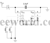 Figure 1 X9511 basic application
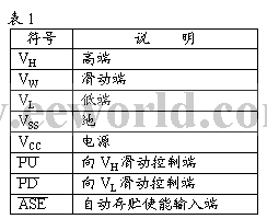 3 Problems often encountered in the application of digital potentiometers Digital potentiometers are still new devices that have appeared in our country in recent years. Many people do not know enough about them in practical applications, resulting in many questions. The following are often Three issues that arise are briefly discussed. For digital potentiometers controlled by buttons, the number of button presses and output values often do not match the predicted values. The digital potentiometer itself can withstand limited current and voltage and needs to be expanded. In practical applications, the resistance range and resolution of digital potentiometers are not enough and need to be expanded. 3.1 The problem of anti-jitter and repeated triggering of the button-controlled digital potentiometer. The first question mentioned above is that the number of key presses and the output value of the button-controlled digital potentiometer are inconsistent with the prediction. Usually, there is a repeated triggering action in one of the gears. Naturally, other The number of key presses and output potential will not match the predicted values. This phenomenon is often caused by using a breadboard for testing, or using inferior buttons, resulting in poor contact, increased line noise, or irregular button actions. If the application circuit of the push-button digital potentiometer provided by the American XICOR company is directly controlled by buttons, these problems may occur. X9511/14 integrates a 40ms delay debounce circuit inside it, which requires the input control signal jitter time to be short, the signal validity time to be between 40ms and 250ms, and no interference level to occur during this period. However, due to the unpredictable actual application conditions, it is impossible to avoid the jitter of the input signal causing repeated movements of the output (the button time exceeding 250ms will also cause repeated movements of the output), which is what many people do not want to see. In order to control the jitter and noise effects of the input signal, a trigger is added to the control end of the digital potentiometer, as shown in Figure 2. The test results have significantly improved the output stability, but the button action is still required to be crisp and crisp, and There is no interference in the line, and the final performance is that the input signal is clean and has no fluctuations, otherwise repeated triggering cannot be avoided. After many improvements, the circuit in Figure 3 has better solved the above problems. Between the button and the control input terminal, a monostable circuit composed of a NAND gate circuit is added as shown in Figure 3. It has the characteristics of low cost, simple circuit, can prevent jitter, and will not cause the output to act repeatedly.
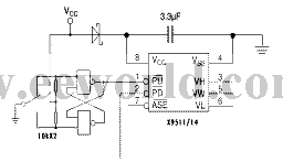 Figure 2 Add anti-shake trigger When button K in Figure 3 is not in action, the control terminal must be at a stable high level. Once the button is pressed, the potential at point A is discharged through capacitor C1 through resistor R1, to the input low level gate of 74HC00 limit, point B is a logic high, and at the same time, point F is used to control the level of point E (point D was originally high level) to flip to low, starting the X9511 action. At this time, because the potential of capacitor C2 will not change immediately, point D Keeping the original high level unchanged, capacitor C2 discharges through R2, and after a transient time reaches the low level threshold of the gate circuit, causing point E to return to high level. Afterwards, no matter whether the button remains pressed (keeping point D low) or released (point F is low), point E will remain high. During the transient period, the low level of point E is locked. Even if the circuit produces strong level jitter at point A, it will not have any impact on the output. Due to the shielding effect of the circuit on noise during the transient time, if the control terminal is low-level
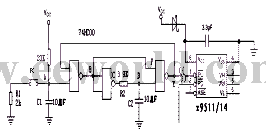 for more than 250ms, the output of X9511/14 will continuously jump. Therefore, the R2 value can be adjusted to control the transient time within a range where the non-repetitive action time of the X9511 is as long as possible (for example, the transient time can be between 150ms and 220ms) to shield possible noise interference during this period. The values of R2 and C2 can be obtained according to the formula of transient time T. T=(R2+R0)·C2·Ln[(Vol-Voh) / (Vol-Vth)] where R0 is the output resistance of 74HC00; Vol is the low-level output voltage of 74HC00; Voh is the high-level voltage of 74HC00 Output voltage; Vth is the high-level flip threshold voltage of 74HC00
 Figure 1 X9511 basic application
 3 Problems often encountered in the application of digital potentiometers Digital potentiometers are still new devices that have appeared in our country in recent years. Many people do not know enough about them in practical applications, resulting in many questions. The following are often Three issues that arise are briefly discussed. For digital potentiometers controlled by buttons, the number of button presses and output values often do not match the predicted values. The digital potentiometer itself can withstand limited current and voltage and needs to be expanded. In practical applications, the resistance range and resolution of digital potentiometers are not enough and need to be expanded. 3.1 The problem of anti-jitter and repeated triggering of the button-controlled digital potentiometer. The first question mentioned above is that the number of key presses and the output value of the button-controlled digital potentiometer are inconsistent with the prediction. Usually, there is a repeated triggering action in one of the gears. Naturally, other The number of key presses and output potential will not match the predicted values. This phenomenon is often caused by using a breadboard for testing, or using inferior buttons, resulting in poor contact, increased line noise, or irregular button actions. If the application circuit of the push-button digital potentiometer provided by the American XICOR company is directly controlled by buttons, these problems may occur. X9511/14 integrates a 40ms delay debounce circuit inside it, which requires the input control signal jitter time to be short, the signal validity time to be between 40ms and 250ms, and no interference level to occur during this period. However, due to the unpredictable actual application conditions, it is impossible to avoid the jitter of the input signal causing repeated movements of the output (the button time exceeding 250ms will also cause repeated movements of the output), which is what many people do not want to see. In order to control the jitter and noise effects of the input signal, a trigger is added to the control end of the digital potentiometer, as shown in Figure 2. The test results have significantly improved the output stability, but the button action is still required to be crisp and crisp, and There is no interference in the line, and the final performance is that the input signal is clean and has no fluctuations, otherwise repeated triggering cannot be avoided. After many improvements, the circuit in Figure 3 has better solved the above problems. Between the button and the control input terminal, a monostable circuit composed of a NAND gate circuit is added as shown in Figure 3. It has the characteristics of low cost, simple circuit, can prevent jitter, and will not cause the output to act repeatedly.
 Figure 2 Add anti-shake trigger When button K in Figure 3 is not in action, the control terminal must be at a stable high level. Once the button is pressed, the potential at point A is discharged through capacitor C1 through resistor R1, to the input low level gate of 74HC00 limit, point B is a logic high, and at the same time, point F is used to control the level of point E (point D was originally high level) to flip to low, starting the X9511 action. At this time, because the potential of capacitor C2 will not change immediately, point D Keeping the original high level unchanged, capacitor C2 discharges through R2, and after a transient time reaches the low level threshold of the gate circuit, causing point E to return to high level. Afterwards, no matter whether the button remains pressed (keeping point D low) or released (point F is low), point E will remain high. During the transient period, the low level of point E is locked. Even if the circuit produces strong level jitter at point A, it will not have any impact on the output. Due to the shielding effect of the circuit on noise during the transient time, if the control terminal is low-level
 for more than 250ms, the output of X9511/14 will continuously jump. Therefore, the R2 value can be adjusted to control the transient time within a range where the non-repetitive action time of the X9511 is as long as possible (for example, the transient time can be between 150ms and 220ms) to shield possible noise interference during this period. The values of R2 and C2 can be obtained according to the formula of transient time T. T=(R2+R0)·C2·Ln[(Vol-Voh) / (Vol-Vth)] where R0 is the output resistance of 74HC00; Vol is the low-level output voltage of 74HC00; Voh is the high-level voltage of 74HC00 Output voltage; Vth is the high-level flip threshold voltage of 74HC00
 Latest Basic Circuits Circuits
- What is the difference between CPLD and FPGA?
- Diode-based clipping circuit
- Beautiful crown wreath made with LED
- Share an interesting LED decoration project
- What is a Demultiplexer
- Touch circuit design and analysis
- Digital number selection machine
- FL52C4 induction electronic greeter
- NE5532 standard linear preamplifier IC circuit features and application schematics
- Using Monostable Trigger to Construct Pulse Delay Circuit
Popular Circuits
- 555 square wave oscillation circuit
- 555 photo exposure timer circuit diagram
- Introducing the CD4013 washing machine timer circuit diagram
- Simple level conversion circuit diagram
- 555 electronic guide speaker circuit diagram for blind people
- Circuit diagram of disconnection alarm composed of 555
- Analog circuit corrector circuit diagram
- color discrimination circuit
- Color sensor amplification circuit
- Level indication circuit


 京公网安备 11010802033920号