85% of the information in the world today is stored in hard drives. Have you ever thought that one day, even if the hard drive is full, it will not be able to save the current data?
It’s hard to imagine that from 1971 to 1996, people were still using magnetic floppy disks that were only 1.44MB. Now, although NAND Flash is king, people can save more and more, and read faster and faster, but they are also encountering bottlenecks. As process technology approaches 1nm, it becomes increasingly difficult to increase hard drive capacity. People continue to "stack" NAND Flash chips in hard drives to increase hard drive capacity from another dimension.But technical bottlenecks still exist, and new technologies are needed at this time. The technology that has attracted much attention is MRAM (magnetoresistive memory). Yes, that’s right, people are going round and round and putting their hopes on “magnetic”.This article is the first article in the "Primary Market" topic, focusing on the development of MRAM international giants and domestic entrepreneurship.
Fu Bin丨Author
Produced by Electronic Engineering World (ID: EEworldbbs)丨
In fact, in addition to the memory (DRAM) and SSD (NAND Flash) that we are familiar with, scientists and the industry have always wanted to replace the memory and hard drive in your computer, because they are not perfect technologies. Either the power is cut off and the data is lost, or the storage is relatively slow. slow.For this reason, new types of storage emerged. New memories mainly include four types: resistive memory (ReRAM/RRAM), phase change memory (PCM), ferroelectric memory (FeRAM/FRAM), and magnetic memory (MRAM).

Comparison of main new storage parameters, tabulation丨Electronic Engineering WorldMRAM is a very important type of new storage and is very close to the industry. Simply put, it is stronger and faster. However, there are no hexagon warriors in the storage world, so it all depends on what the application needs and what technology to choose.

Comprehensive comparison chart of four types of new non-volatile memories and NAND Flash indicators, source | Technology ChinaMRAM is a non-volatile storage technology. It is called an "all-rounder" because, as the name suggests, MRAM can do a little bit of everything.Although SRAM is fast, its capacity is extremely low; DRAM has a simple structure, but is also trapped by volatility; non-volatile, large-capacity Flash has limited durability, and as the manufacturing process gradually approaches the limit, it will reach the limit indefinitely.MRAM has speed and area between the two volatile storage technologies of SRAM and DRAM. It also has the characteristics of unlimited read and write times, fast writing speed, low power consumption, radiation resistance and high integration of logic chips. In addition, the current temperature resistance of MRAM laboratories can reach -40℃~150℃, covering the -40℃~120℃ of automotive chips.
Of course, MRAM is not without its shortcomings. It also faces many challenges, such as the complex material system of the real device, low switching ratio, and the CMOS process must be fully matched. In addition, the development of MRAM still encounters bottlenecks in dynamic power consumption, energy delay efficiency and reliability.
 Unlike traditional RAM, MRAM does not store data using charges or currents, but magnetically stores data using MTJ (Magnetic tunnel junction).
Now, there are various structures of MTJ, which is where MRAM becomes complicated.

Different MTJ types, picture source丨Shanghai Institute of Microsystems and Information Technology, Chinese Academy of SciencesCurrently, MRAM is divided into three generations: the first generation is MRAM, which is called magnetic field driven MRAM; the second generation is STT-RAM (spin transfer torque), which causes the magnetic moment to flip by passing a current perpendicular to the tunnel junction; the third generation Modern MRAM technology is divided into two types, namely spin-orbit moment MRAM (SOT-MRAM), which causes the magnetic moment to flip by passing an in-plane current in the heavy metal layer, and changes the magnetic anisotropy by applying a voltage to cause the magnetic moment to flip. The flipped one is called Voltage Controlled Magnetic Anisotropic MRAM (VCMA-MRAM or MeRAM).MRAM has a long history of development and has many applications in the field of IoT embedded storage. In recent years, STT-MRAM based on spin torque transfer has become mainstream, and the third generation of SOT-MRAM is gradually being industrialized.The application scenario of MRAM is mainly to replace some existing storage technologies. For example, it can be used to replace DRAM or SRAM so that it can save data even when the power is off. MRAM has obvious advantages in reading and writing speed and durability.In the industrial field, applications require very fast writing capabilities and non-volatile storage, but NAND, NOR and EEPROM are slow to write, consume a lot of power, and require additional SRAM with batteries. At this time, the advantages of MRAM are reflected Out.Nowadays, with the rise of autonomous driving and AI, faster computing and stronger computing power are required for storage and calculation. This requires embedding memory into processing chips (such as MCU), so as to transmit data over extremely short distances (nanometers to microns). level) to achieve near-memory computing.
MRAM is highly compatible with CMOS in terms of technology. One metal layer can be used as MRAM and other metal layers can be used as processors and logic circuits. It is easy to achieve extremely short data transmission distances on the order of nanometers to micrometers, thereby increasing the computing power of AI calculations. Improved by orders of magnitude. Therefore, automatic driving and automotive electronics are excellent application scenarios for MRAM.

Can the country seize new opportunities?
MRAM undoubtedly has "money prospects". Many experts predict that MRAM will bring about the next wave of storage.Menafn reports show that the MRAM market will explode from now on, and is expected to be worth US$19.1893 billion by 2031, with a compound annual growth rate of 36.6% from 2021 to 2031. The automotive market and the Internet of Things market are areas where MRAM has the highest growth momentum.Yole Developpement predicts that between 2020 and 2026, the overall emerging non-volatile memory (NVM) market will have a compound annual growth rate of approximately 44%. As emerging embedded NVM technology matures significantly, the eMRAM market size is estimated to be 1.7 billion in 2026 USD, accounting for approximately 76% of the overall emerging eNVM market.Internationally, MRAM has always been highly concerned, and some landmark events include:· In the 1980s, molecular beam epitaxy equipment entered France;· In 1988, Fair's team discovered the giant magnetoresistance effect;· In 1990, IBM began to use this effect to develop large-capacity hard drives;· In 1997, giant magnetoresistive hard drives were put into commercial use. So far, the data storage capacity has increased by more than 100,000 times;· In 2008, Freescale established EverSpin to promote MRAM business;· In 2012, Everspin announced the world’s first STT-MRAM chip and began providing it to customers in 2013;· The American company Everspin released a commercial STT-MRAM chip with a capacity of 1GB in 2018;· South Korea’s Samsung Company has mass-produced embedded MRAM (eMRAM) on its 28nm FD-SOI process production line;· Intel has launched a new type of MRAM that can increase storage space by 20 times and is 20 times faster than traditional DRAM;· In 2014, Everspin announced it would increase production and the company disclosed several new customer and ecosystem relationships;· In 2019, Western Digital adopted spin oscillation writing technology (MRAM) to increase capacity by another 10 to 20 times;· In June 2022, the low-voltage current SOT-MRAM jointly developed by Taiwan Industrial Research Institute and TSMC has the characteristics of high writing efficiency and low writing voltage. Its SOT-MRAM achieved a writing speed of 0.4 nanoseconds and a write speed of 70,000 The high endurance of 100 million reads and writes can also provide a data storage life of more than 10 years;· In October 2022, Samsung Research realized the manufacturing of magnetic tunnel junction stacked magnetoresistive random access memory (MRAM) on the 14nm FinFET logic process platform. It is said to be the smallest and lowest power non-volatile memory in the world. sexual memory;· In May 2023, NXP Semiconductors announced that it would cooperate with TSMC to launch the industry’s first automotive embedded magnetoresistive random access memory (MRAM) using 16nm fin field effect transistor (FinFET) technology.
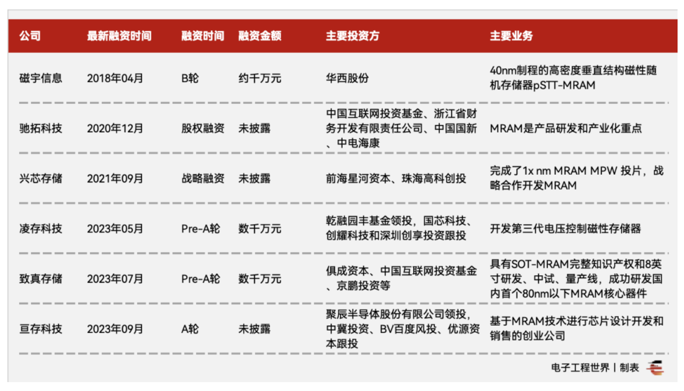
China explored magnetic memory earlier. As early as the late 1950s and early 1960s, domestic research and development for the industrialization of storage technology started. Although there was no such concept as MRAM at that time, the magnetic core storage technology that imitated Soviet computers at that time could be called It is the earliest MRAM.According to incomplete statistics from EEworld, the performance of Ciyu Information, Chituo Technology, Xingxin Storage, Lingcun Technology, Zhizhen Storage, and Ecun Technology is worthy of attention, especially the latter three companies, which have made many moves recently.
· In August 2023, the 128Kb SOT-MRAM chip independently developed by Zhizhen Memory successfully rolled off the production line. It is another important milestone in the development of a new generation of magnetic storage technology after the successful tape-out of 1Kb SOT-MRAM. It revolves around spin-orbit moment materials. , magnetic tunnel junction patterning, special circuit design, etc. to achieve many technological breakthroughs;· In response to the intelligent needs of the edge and end sides, Gencun Technology has laid out two core product lines of "independent MRAM memory chips" and "AI SoC chips" including embedded MRAM around "storage-computing-control" to provide consumers with Provide competitive, energy-efficient, intelligent single-chip series solutions to customers in , industry, Internet of Things, automotive and other fields. Among them, the "ultra-low power consumption" version of the AI SoC has an operating power consumption as low as 5uA/MHz, reaching the world's first-class level, and can provide a cost-effective solution for a wide range of battery-powered application scenarios;· Lingcun Technology has successfully developed the world's first high-speed, high-density, low-power memory MeRAM prototype and a MeRAM-based true random number generator. The high-performance memory chips it developed are widely used in automotive electronics and high-performance computing , security and other fields, it also licenses storage media, integrated circuits, systems and related patents to companies with needs for efficient computing and security chips to develop related products on their own;· Ciyu Information is a company that owns pSTT-MRAM dedicated 12-inch thin film manufacturing/testing equipment and pSTT-MRAM dedicated 12-inch etching equipment. Foreign MRAM is mainly used in solid-state drives to achieve a significant improvement in the performance of solid-state drives. This is also the reason for magnetic The starting point of Yu information products;· Chituo Technology has also had customers mass-produced embedded non-volatile memory for MCU/SOC and slow SRAM;· Zhuhai Xingxin Storage (a wholly-owned subsidiary of Zhuhai Antarctica Technology) has NV-RAM specification MRAM technology. It is the first domestic manufacturer to achieve this specification. After mass production in the future, it can replace the expensive FRAM and FRAM currently supplied by foreign companies on the market. Power supply SRAM (BatteryBackup SRAM), NVSRAM;· A team from the Institute of Physics, Chinese Academy of Sciences, developed a magnetic moment-closed nano-annular magnetic tunnel junction as a new MRAM prototype device for memory cells.


 ISO107B


 京公网安备 11010802033920号