The Next-Gen, Software-Defined Radio (SDR) Transceiver Delivers Big Advances in Frequency Hopping (FH)
Next-generation software-defined radio (SDR) transceiver offers significant frequency hopping (FH) advantages
summary
This article takes a deep dive into the concept of frequency hopping (FH) and how the four major frequency hopping features can be achieved through flexible design of the phase-locked loop (PLL) architecture of the ADRV9002 SDR transceiver. These features provide users with powerful frequency hopping capabilities, allowing them to handle applications such as Link 16 and fast real-time carrier frequency loading in single-channel and dual-channel operation modes. In addition, the combination of frequency hopping with multi-chip synchronization (MCS) and digital pre-distortion (DPD) technology makes the ADRV9002 SDR transceiver a very attractive solution to meet the higher requirements in today's complex communication systems.
Introduction
Unlike traditional radio communications, frequency hopping (FH) defines a method of sending radio signals by rapidly changing the carrier frequency1, which was first mentioned by Nikola Tesla in his 1903 U.S. patent "Method for the Transmission of Signals". Later, in 1942, actress Hedy Lamarr and composer George Antheil further solidified the concept by switching between 88 frequencies inspired by the number of keys on a piano to prevent interference with the radio control of torpedoes. Over the past 100 years, the application of frequency hopping in the military field has entered a new era, from non-real-time, low-speed communications between fixed command points in World War I to real-time, high-speed multimedia communications between contemporary aircraft, ships and land systems. In addition, frequency hopping has been widely used in many wireless personal communication networks, such as Bluetooth® Personal Area Networks (PANs), as well as in consumer electronics and amateur radio fields, such as walkie-talkies, car models and drones.
What is Frequency Hopping?
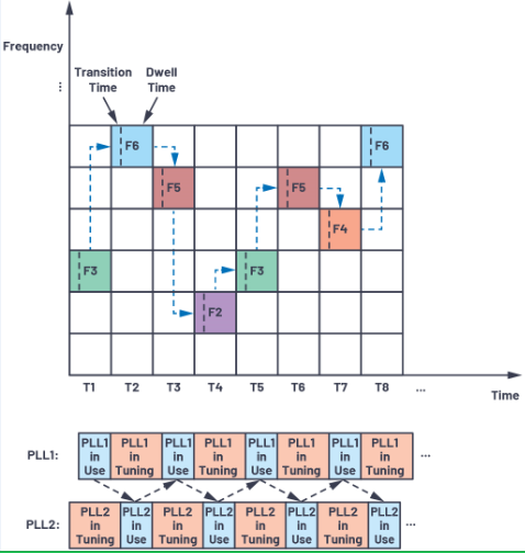
The concept of frequency hopping is shown in Figure 1. If the entire frequency band and duration are divided into a two-dimensional grid, then in any given time slot, different frequency sub-bands will be used for communication. The randomness of the frequency hopping pattern is equivalent to adding another security layer that can only be decoded between the transmitter and the receiver, making it highly resistant to narrowband interference and highly resistant to malicious interception and blocking. In addition, frequency hopping signals have little mutual interference and can share bandwidth with other traditional communications to achieve higher spectral efficiency. As the frequency hopping rate increases and more sub-bands are used, the advantages of frequency hopping become more prominent, becoming an attractive solution for many different applications.

Figure 1. Concept of frequency hopping
Next Generation SDR Transceivers
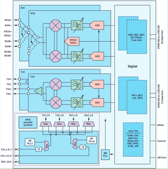
The ADRV9002 is a dual narrowband and wideband SDR transceiver that provides excellent RF performance and advanced system features such as DPD and frequency hopping. The ADRV9002 operates from 30 MHz to 6 GHz, covering the ultra-high frequency (UHF) band; the ultra-high frequency (VHF) band; the industrial, scientific and medical (ISM) band and the cellular band. It can support narrowband (kHz) and wideband operations up to 40 MHz. Figure 2 shows a simplified schematic block diagram of the ADRV9002. It includes dual transmit and receive channels, as well as a set of advanced digital signal processing algorithms. Many other transceivers dedicate one PLL to the receive data path and the other to the transmit data path, while the ADRV9002 PLL structure shown in the red box is unique in that it uses two RF PLLs in the device and can choose to provide both PLLs to any receiver or transmitter, both together or none at all. This flexibility is key to supporting frequency hopping in various TDD applications, such as single-channel and dual-channel operation, including transmit-only mode (1T/2T), receive-only mode (1R/2R), and transmit/receive mode (1T1R/2T2R). Dual-channel operation supports channel diversity and channel multiplexing. In addition, two PLLs can be used in ping-pong mode to meet strict frequency hopping timing requirements.
Four frequency hopping characteristics of ADRV9002
Very fast frequency hopping via two PLL multiplexing and fast PLL retuning
Frequency hopping is achieved by retuning the PLL before switching to a different frequency. The ADRV9002 provides different frequency hopping modes depending on the usage of the PLL. 2 Each time slot in Figure 1 represents a hopping frame, which can be divided into a switching period and a dwell period, as shown in Figure 3.

Figure 2. Simplified block diagram of the ADRV9002 with flexible PLL design.

Figure 3. Frame skipping structure
In the slower frequency hopping mode, if the transition time between frequency changes is long enough (longer than the channel setup time and the required PLL tuning time), only one PLL is needed for a pair of transmit and receive channels in TDD operation (called one PLL retuning mode). To achieve faster frequency hopping and shorter transition times (shorter than the channel setup time and the required PLL tuning time), two phase-locked loops can be used in the device (called two PLL multiplexing mode). The two PLLs coordinate with each other in a ping-pong manner: while one PLL is used for the current frequency, the other PLL is retuned to the next frequency. This allows fast frequency hopping, which greatly reduces the required transition time between different frequency changes. Table 1 summarizes these two modes.
Table 1. ADRV9002 Frequency Hopping Modes (Based on PLL Usage)

As shown in Table 1, the selection of one of the two modes is determined by the user-defined transition time.
Figure 4 further explains the PLL multiplexing mode concept. As mentioned earlier, each time slot represents a skip frame, which consists of a switching period and a dwell period. When one PLL is used during the dwell time, the other PLL starts tuning from the beginning of the switching time of the same skip frame. It can keep tuning until the end of the switching period of the next skip frame. Therefore, as long as the required PLL tuning time is shorter than the sum of one dwell time and two switching times, the PLL multiplexing mode is successful.

Figure 4. PLL multiplexing mode for fast frequency hopping
Frequency hopping in PLL multiplexing mode is critical for military applications such as Link 16. Link 16 is considered one of the most important tactical data link standards used by the North Atlantic Treaty Organization (NATO) and uses an interference-resistant, high-speed digital data link in the 960 MHz to 1.215 GHz RF band. 3 The ADRV9002 uses a fast PLL re-tuning mode to meet stringent timing requirements by accurately calibrating the entire frequency hopping range at initialization. The PLL re-tuning time depends on the ADRV9002 PLL reference clock rate. Table 2 shows the fast PLL re-tuning time required at different PLL reference clock rates. The fast PLL re-tuning time is approximately 15 μs for a PLL reference clock rate of 300 MHz. With a Link 16 frame hopping length of 13 μs, if the transition time is greater than 2 μs, a PLL re-tuning time of 15 μs can meet the timing requirements when using PLL multiplexing mode, as shown in Table 1.
Table 2. PLL retuning time when using fast PLL retuning mode

As described in the paper “Performance Analysis of JTIDS/Link 16-Type Waveforms Transmitted over Slow, Flat Nakagami Fading Channels in the Presence of Narrowband Interference”3, Link 16 message data can be sent as a single pulse or dual pulse, depending on the packetization structure. The single pulse structure consists of a 6.4 μs on time and a 6.6 μs off time, for a total duration of 13 μs. The dual pulse structure consists of two single pulses that transmit the same data but use different carrier frequencies, as shown in Figure 5. Therefore, the transition time is approximately 6.6 μs (>2 μs), making it entirely feasible to implement Link 16 frequency hopping using the ADRV9002.

Figure 5. Standard Link 16 dual pulse structure
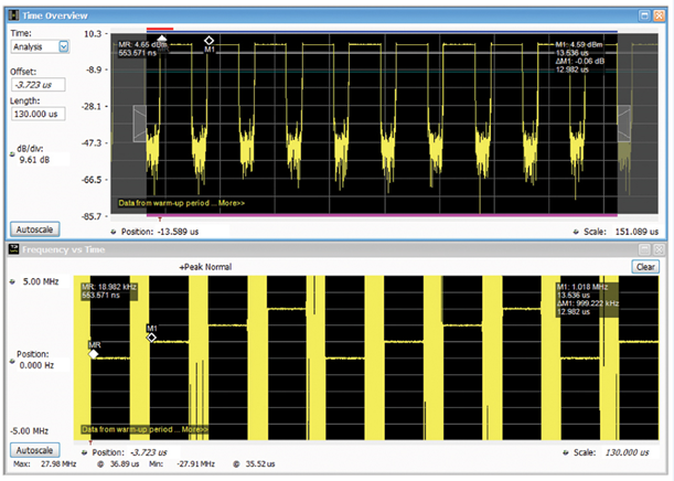
Figure 6 shows the ADRV9002 transmit output (power vs. time and frequency vs. time) with Link 16 type frame hopping (for simplicity, only transmit frequency hopping is used). Note that in order to show the minimum transition time achievable with the ADRV9002, the experiment did not use the standard Link 16 pulse structure shown in Figure 5, but instead the on time was increased from 6.4 μs to 11 μs and the off time was decreased from 6.6 μs to 2 μs. A Tektronix RSA306B spectrum analyzer was connected to the transmit output port of the ADRV9002 evaluation board for observation. The upper plot shows power vs. time. It can be seen that the transmit frequency hopping occurs every 13 μs, with a transition time of approximately 3 μs between consecutive transmit frame hopping. The lower plot shows frequency vs. time. In this experiment, the transmit carrier frequency cycles between four different frequencies in 1 MHz steps. As expected, the lower plot confirms that the transmit output also cycles between four different frequencies in 1 MHz steps with excellent frequency accuracy throughout the dwell period.

Figure 6. Link 16 Tx frequency hopping transmit output
The frequency accuracy of Link 16 frequency hopping can be further measured by using more advanced test equipment such as Keysight E5052B and R&S FSWP. In the measurement example shown in Table 3, the transmit carrier frequency hops at 400 MHz, 400.1 MHz, 400.2 MHz, and 400.3 MHz. The transmit input signal also changes frequency synchronously to generate a frequency output of 400 MHz for all hopping frames. The measurement duration is set to 100 μs, which includes 7 complete hopping frames. The frequency is measured every 128 ns. It can be seen that the PLL is fully locked at the beginning of the dwell time. The frequency error during the dwell time depends on the phase noise performance. Table 3 shows the average, maximum, and minimum frequency offset (absolute difference between the output frequency and 400 MHz) performance of these 7 consecutive hopping frames. In most frames, the average frequency error is less than 1 ppm. Dozens of experiments show the same results. Note that the measured values may vary depending on the equipment and test configuration.
Previous article:Native apps, web apps, hybrid apps, and progressive web apps: the best app is the one that suits your needs
Next article:Qualcomm launches next-generation power line communications products to meet growing demand for smart grid communications from vehicle to charging station
Recommended ReadingLatest update time:2024-11-16 14:25


- Popular Resources
- Popular amplifiers
-
 New concept analog circuit 1-5
 -
 Convex Optimization in Signal Processing and Communications: From Foundations to Applications (Qi Zhongyong, Li Weichang, Lin Jiaxiang)
 -
 \"New Concept Analog Circuit\" - Transistor [Text Version] (Yang Jianguo)
 -
 ADI Technical Tutorial Collection - Circuit Simulation and PCB Design
- Wi-Fi 8 specification is on the way: 2.4/5/6GHz triple-band operation
- Three steps to govern hybrid multicloud environments
- Microchip Accelerates Real-Time Edge AI Deployment with NVIDIA Holoscan Platform
- Keysight Technologies FieldFox handheld analyzer with VDI spread spectrum module to achieve millimeter wave analysis function
- Qualcomm launches its first RISC-V architecture programmable connectivity module QCC74xM, supporting Wi-Fi 6 and other protocols
- Microchip Launches Broadest Portfolio of IGBT 7 Power Devices Designed for Sustainable Development, E-Mobility and Data Center Applications
- Infineon Technologies Launches New High-Performance Microcontroller AURIX™ TC4Dx
- Rambus Announces Industry’s First HBM4 Controller IP to Accelerate Next-Generation AI Workloads
- NXP FRDM platform promotes wireless connectivity
- Innolux's intelligent steer-by-wire solution makes cars smarter and safer
- 8051 MCU - Parity Check
- How to efficiently balance the sensitivity of tactile sensing interfaces
- What should I do if the servo motor shakes? What causes the servo motor to shake quickly?
- 【Brushless Motor】Analysis of three-phase BLDC motor and sharing of two popular development boards
- Midea Industrial Technology's subsidiaries Clou Electronics and Hekang New Energy jointly appeared at the Munich Battery Energy Storage Exhibition and Solar Energy Exhibition
- Guoxin Sichen | Application of ferroelectric memory PB85RS2MC in power battery management, with a capacity of 2M
- Analysis of common faults of frequency converter
- In a head-on competition with Qualcomm, what kind of cockpit products has Intel come up with?
- Dalian Rongke's all-vanadium liquid flow battery energy storage equipment industrialization project has entered the sprint stage before production
- Allegro MicroSystems Introduces Advanced Magnetic and Inductive Position Sensing Solutions at Electronica 2024
- Car key in the left hand, liveness detection radar in the right hand, UWB is imperative for cars!
- After a decade of rapid development, domestic CIS has entered the market
- Aegis Dagger Battery + Thor EM-i Super Hybrid, Geely New Energy has thrown out two "king bombs"
- A brief discussion on functional safety - fault, error, and failure
- In the smart car 2.0 cycle, these core industry chains are facing major opportunities!
- The United States and Japan are developing new batteries. CATL faces challenges? How should China's new energy battery industry respond?
- Murata launches high-precision 6-axis inertial sensor for automobiles
- Ford patents pre-charge alarm to help save costs and respond to emergencies
- New real-time microcontroller system from Texas Instruments enables smarter processing in automotive and industrial applications
- 【ST NUCLEO-H743ZI Review】(2) First experience with Ethernet testing
- Disassembling a common fire emergency light
- [NXP Rapid IoT Review] Mobile APP connection finally succeeded
- Buy an oscilloscope and get the essential analysis software 5-PWR for power engineers
- Analysis of common problems of touch switches
- Which power chip is BNOF?
- The 2019 TI Industrial Applications Seminar is coming, and the Ningbo special session is waiting for you to sign up!
- [ST NUCLEO-H743ZI Review] Try to play with DAC2ADC
- GPS signal acquisition problem under ZSTACK protocol stack
- Active and passive cell balancing for battery packs


 New concept analog circuit 1-5
 Convex Optimization in Signal Processing and Communications: From Foundations to Applications (Qi Zhongyong, Li Weichang, Lin Jiaxiang)


 京公网安备 11010802033920号