TMS320F2812 is the latest generation of C2000 family launched by Texas Instruments. The advanced internal and peripheral structures make this processor mainly used for large storage device management and high-performance control occasions. In the application system composed of F2812, some logic control circuits need to be designed to ensure the normal and orderly operation of the system. Here, we use CPLD to design the decoding and logic control of the peripheral circuit to make the DSP system miniaturized, integrated and highly reliable.
2 Application of CPLD in TMS320F2812 System
2.1 Introduction to TMS320F2812
TMS320F2812 digital signal processor is a high-performance fixed-point chip developed on the basis of F24X. It can run code programs developed by 24x, and F2812 uses 32-bit operation to greatly improve the processing capability. Its main features are as follows:
Using high-performance static CMOS technology, the main frequency can operate at 150 MHZ (clock cycle can reach 6.67ns);
High-performance 32-bit CPU capable of 16-bit x 16-bit and 32-bit x 32-bit multiplication and accumulation operations;
On-chip large-capacity memory, 128K×16 bits of Flash and 18K×16 bits of data/program memory;
High-speed peripheral interface, expandable memory up to 1.5 M×16 bit;
3 32-bit CPU timers, of which CPU timer 1 and CPU timer 2 are reserved for real-time operating system OS. CPU timer 0 is available for users to use as an independent, global timer interrupt control;
12-bit ADC pipeline conversion time is as low as 60 ns, single conversion is 200 ns; two time manager trigger functions can be selected;
Improved eCAN 2.0B interface module;
Multiple serial communication interfaces (2 UARTs, 1 SPI and 1 MCBSP);
High performance and low power consumption, using 1.8V core voltage and 3.3V peripheral interface voltage;
2.2 Hardware Structure Introduction
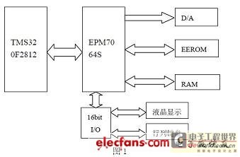
We use Alter's EPM7064S chip to complete internal logic management and bus interface work. The chip uses flash memory technology (FastFLASH) and has low power consumption. The number of macro units reaches 64, which fully meets the logic requirements of the design. The pin-to-pin delay is 4ns, and the counter frequency can reach 151MHZ. Its output voltage is 3.3V or 5V, and different output voltages can be selected by setting the VCCIO pin. The I/O pin can accept mixed voltage inputs of 5V, 3.3V and 2.5V. In multi-power mixed systems, this feature is very useful and can save a lot of level converters.
The TMS320F2812 application system needs to expand some necessary circuits, including RAM and EEROM to support the internal program running, as well as D/A conversion circuits, etc. The system structure block diagram is shown in Figure 1:

[page]
2.2.1 Application of Digital-to-Analog Converters
In TMS320F2812, off-chip expansion is achieved through the peripheral interface XINTF in TMS320F2812.
It is similar to the external interface of C240X, but also has some improvements:
(1) In C240X, program storage space, data storage space and I/O space are mapped at the same address (0000~FFFF), and access to them is distinguished by control lines (DS, PS, IS); in F2812, the external memory interface is divided into 5 fixed memory map areas, which can address 1MB of off-chip memory space with independent addresses and no control lines (DS, PS, IS).
(2) Each XINTF area of F2812 has a chip select signal. Among them, the chip select signals of some areas are internally "ANDed" together to form a shared chip select, such as XZCS0 and XZCS1 share a chip select signal XZCS0AND1, and XZCS6 and XZCS7 share a chip select signal XZCS6AND7. In this way, the same memory can be connected to two areas or we can use external decoding logic to distinguish the two areas.
(3) Each of the five fixed memory image areas can also specify the number of wait states, the setup time, activation time and hold time of the selection signal. These features make the interface disconnected from the external memory and peripherals, and can be flexibly and independently expanded externally. In this design, except for the LCD display module and keyboard, all external expansion registers and memories are mapped in the decoding space of XINTFZONE 2 (0x080000~0x0FFFFF). We used DAC7625 as the digital-to-analog conversion chip, which is a 4-channel 12-bit double-buffered DAC chip, and the operating voltage can be +5V or -5V~+5V analog voltage.
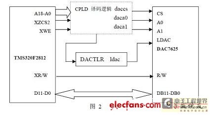
The output voltage is a DC voltage of 0 to 3.3V. The functional block diagram is shown in Figure 2:

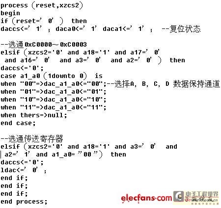
Among them, the LDAC pin in the DAC7625 chip is the loading DAC pin. When it is low, all registers are transparent, and the data in the holding register is sent to the converter output channel; the A1 and A0 pins are register selection pins. The CPLD selects different A1 and A0 combinations according to the address bus decoding, thereby mapping the holding registers of channels 1 to 4 to the address space of 0xC0000~0xC0003. In addition, we also designed a transfer register (DACTLR) with a mapping address of 0xC0004. All data bits of this register are invalid and cannot be read or written. Any read or write operation on this register will generate an internal signal, set the LDAC pin to a low level, and start the converter. Among them, the entire decoding logic is completed by the CPLD chip. The following is a partial VHDL language description of the decoding logic:

2.2.2 Application of Serial Non-Volatile Memory X25650 Chip
Here, we expand the SPIOER register to control the SPI interface between DSP and X25650. Its function is to connect or disconnect the connection between DSP and X25625. When the SPI interface of F2812 needs to be connected to the SPI515 (SPI interface type) simulator to realize simulation operation, the operation of SPI to X25650 can be shielded through the register. The address of the SPIOER control register is 0xC0002, and the external bus is used to read and write it. Its use:
SPIOE bit: When the SPIOE bit is "1", the DSP is connected to each pin of X25650; when it is "0", each pin is disconnected. At this time, the SPI pin on the DSP is in high impedance state and can be connected to other devices. It is "1" when power-on reset. This register is composed of CPLD internal programming.
In F2812, the SPI module supports 125 different baud rates. By writing the set value to the baud rate register (SPIBRR), it can communicate with peripherals with different speed requirements. The baud rate settings are as follows:

When SPIBRR = "3-127", SPI baud rate = LSPCLK/(SPIBRR+1). When SPIBRR = 0, 1, 2, SPI baud rate = LSPCLK/4 Here: LSPCLK = low speed peripheral clock frequency of the device. SPIBRR = content of SPIBRR in the master SPI device.
Here, by configuring the contents of the low-speed peripheral clock prescaler register (LOSPCP) and the SPI baud rate register (SPIBRR), the DSP baud rate reaches 5MHZ, meeting the requirements of X25650.
2.2.3 Application of Character LCD
This system uses the character LCD MDL(S)16263 as a slow display device of DSP, mapped in the XZCS6 area. The module has 11 signal lines. RS is the register selection. Low level selects the instruction register and high level selects the data register. R/W is the read/write control terminal. Low level writes the display module and high level reads the display module. E is the input enable signal line (data read/write operation enable signal), which is valid at high level. DB0~DB7 are data lines.
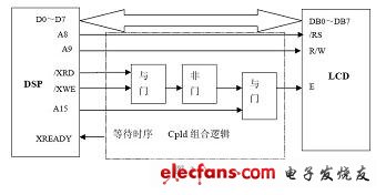
However, compared with DSP, LCD is a slow device. When designing the device, we need to consider the timing matching problem and add appropriate waiting states. The minimum read and write cycle Tcyc of the LCD module is 1000ns, the minimum pulse width Pw is 450ns, and the minimum read and write operation data retention time is 10ns. The read and write access of the XINTF peripheral interface of F2812 is the maximum value by default, which is 26 XTIMCLK cycles (XTIMCLK defaults to SYSCLK/2, 13ns.), that is, the maximum read and write cycle is 346ns, of which the default setting phase of read or write access is 6 XTIMCLK cycles, the default activation phase is 14 XTIMCLK cycles, and the default tracking phase is 6 XTIMCLK cycles. Therefore, the read and write cycles need to add waiting states.
When the XREADY pin of the DSP is sampled as low, the activation phase will extend one XTIMCLK cycle, and XREADY will be sampled again during the next XTIMCLK cycle. This process is sampled until XREADY is sampled as high, and the access is completed normally. Here, we use the CPLD chip to set the XREADY signal of the DSP to a low level and maintain it for 50 XTIMCLK cycles, thereby generating a suitable wait state. As shown in Figure 3:

3 Conclusion
The development of this system adopts the structure of DSP+CPLD, which combines the strong data computing ability of DSP with the high integration and hardware reprogrammability of CPLD, making the design process of the system more reasonable, compact and simplified. Moreover, after expansion, the system can be applied to various occasions of industrial control and has certain practical reference value.
Previous article:FPGA implementation of timing synchronization in OFDM underwater acoustic communication system
Next article:Implementation of multi-tone parallel modulation based on DSP platform
Recommended ReadingLatest update time:2024-11-16 19:38


- Popular Resources
- Popular amplifiers
-
 Learn CPLD and Verilog HDL programming technology from scratch_Let beginners easily learn CPLD system design technology through practical methods
 -
 Practical Electronic Components and Circuit Basics (4th Edition)_Explanation of basic circuit principles, introduction to electronic components, design of various circuits and practical circuit analysis
 -
 FPGA Principle and Structure (Zhao Qian)
 -
 EDA Technology Practical Tutorial--Verilog HDL Edition (Sixth Edition) (Pan Song, Huang Jiye)
- Huawei's Strategic Department Director Gai Gang: The cumulative installed base of open source Euler operating system exceeds 10 million sets
- Analysis of the application of several common contact parts in high-voltage connectors of new energy vehicles
- Wiring harness durability test and contact voltage drop test method
- Sn-doped CuO nanostructure-based ethanol gas sensor for real-time drunk driving detection in vehicles
- Design considerations for automotive battery wiring harness
- Do you know all the various motors commonly used in automotive electronics?
- What are the functions of the Internet of Vehicles? What are the uses and benefits of the Internet of Vehicles?
- Power Inverter - A critical safety system for electric vehicles
- Analysis of the information security mechanism of AUTOSAR, the automotive embedded software framework
 Professor at Beihang University, dedicated to promoting microcontrollers and embedded systems for over 20 years.
- Innolux's intelligent steer-by-wire solution makes cars smarter and safer
- 8051 MCU - Parity Check
- How to efficiently balance the sensitivity of tactile sensing interfaces
- What should I do if the servo motor shakes? What causes the servo motor to shake quickly?
- 【Brushless Motor】Analysis of three-phase BLDC motor and sharing of two popular development boards
- Midea Industrial Technology's subsidiaries Clou Electronics and Hekang New Energy jointly appeared at the Munich Battery Energy Storage Exhibition and Solar Energy Exhibition
- Guoxin Sichen | Application of ferroelectric memory PB85RS2MC in power battery management, with a capacity of 2M
- Analysis of common faults of frequency converter
- In a head-on competition with Qualcomm, what kind of cockpit products has Intel come up with?
- Dalian Rongke's all-vanadium liquid flow battery energy storage equipment industrialization project has entered the sprint stage before production
- Allegro MicroSystems Introduces Advanced Magnetic and Inductive Position Sensing Solutions at Electronica 2024
- Car key in the left hand, liveness detection radar in the right hand, UWB is imperative for cars!
- After a decade of rapid development, domestic CIS has entered the market
- Aegis Dagger Battery + Thor EM-i Super Hybrid, Geely New Energy has thrown out two "king bombs"
- A brief discussion on functional safety - fault, error, and failure
- In the smart car 2.0 cycle, these core industry chains are facing major opportunities!
- The United States and Japan are developing new batteries. CATL faces challenges? How should China's new energy battery industry respond?
- Murata launches high-precision 6-axis inertial sensor for automobiles
- Ford patents pre-charge alarm to help save costs and respond to emergencies
- New real-time microcontroller system from Texas Instruments enables smarter processing in automotive and industrial applications
- cc2531-usbDongle communicates with PC (similar to serial port debugging assistant)
- PCB grounding design specifications worth seeing!
- Serial port screen selection sharing
- How to modify the servo arm? ! ! Please help! !
- Can you guys give me some suggestions, and diagrams?
- The running light delay is realized by the single-chip timer, and the running light style is changed by external interrupt
- Implementation of a Super-resolution Direction Finding Algorithm for Spatial Spectrum Estimation Based on High-speed DSP Series Processors
- IAR FOR MSP430 V7 simulation problem, please solve
- IR2104 drive circuit HO no waveform
- TI C6000 CodecEngine integrated algorithm core calling principle

 Learn CPLD and Verilog HDL programming technology from scratch_Let beginners easily learn CPLD system design technology through practical methods


 京公网安备 11010802033920号