1 Introduction
FPGA is the abbreviation of Field Programming Gate Array. Users can write programs to reconfigure the logic modules and I/O modules inside the FPGA to realize the logic functions of the chip. In recent years, FPGA chips have been widely used for their large scale, high integration, high reliability, low investment, good confidentiality, convenient development, flexible use, and online programming. With the application of FPGA circuits in the military and aerospace fields, their high reliability is particularly important. In order to improve the reliability of the circuit, the best way is to screen the circuit, and the aging test is one of the most important links in the screening process.
Considering that the working mode of FPGA circuit is relatively complex, external memory or FLASH is required to configure it so that FPGA can work dynamically. Therefore, the general FPGA aging technology in China adopts the static aging test method. This static aging test method has certain defects. The circuit is not subjected to real stress during the aging process, so it cannot really eliminate the early failed products, and its reliability cannot be guaranteed. Research on dynamic aging of FPGA circuits can improve the severity of aging test conditions to ensure the high reliability requirements of the circuit.
2 Dynamic aging test
In theory, the dynamic aging of integrated circuits requires that the circuit fully simulate the actual working state under its highest temperature working condition, and the logic units inside the circuit have the opportunity to be flipped. For general digital integrated circuits, external functional test codes are required to drive the circuit to work.
For the dynamic aging test of FPGA circuits, the functional test code is a configuration program stored in an external memory. The program is configured inside the FPGA circuit to make all the internal gate arrays work, achieve high coverage of logic node flipping, and make it work according to the specified functions. Therefore, the key to this research work is how to configure the program of the FPGA circuit.
3 FPGA Design Process
The complete FPGA design process includes logic circuit design input, functional simulation, synthesis and timing analysis, implementation, loading configuration, and debugging. FPGA configuration is the process of converting a specific application design into a data bit stream according to the FPGA design process and loading it into the internal memory of the FPGA to implement a specific logic function. Since the internal memory of the FPGA circuit is based on RAM technology, when the power of the FPGA circuit is turned off, the bit stream data loaded in the internal memory will be lost. Therefore, the designed FPGA bit stream data is usually stored in the external memory, and the FPGA circuit configuration is automatically loaded every time the power is turned on.
4 FPGA Configuration Principles
Taking Xilinx's Qpro VirtexHi-Rel series XQV100 circuit as an example, there are four FPGA configuration modes to choose from: MasterSerial Mode, SlaveSerialMode, Master selectMAPMode, Slave selectMAPMode. Configuration is completed through a set of dedicated/multiplexed pin signals on the chip. The main configuration function signals are as follows:
(1) M0, M1, M2: Download configuration mode selection;
(2) CLK: Configuration clock signal;
(3) DONE: Display configuration status and control device startup;
(4) PROG_B: Initialization pin;
(5) INT_B: Configuration delay control, configuration error display;
(6) DOUT: Configuration data output in daisy chain.
(7) DIN: Serial data input;
The configuration process of the FPGA circuit in the selected mode consists of four main stages:
(1) Clear the FPGA circuit internal configuration memory;
(2) Initialize the FPGA circuit configuration logic function;
(3) Load the FPGA circuit configuration data stream;
(4) The FPGA circuit configuration is completed and the circuit ready sequence is started.
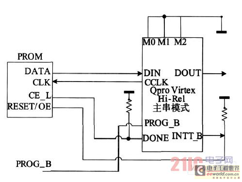
The main series mode circuit connection diagram is shown in Figure 1.

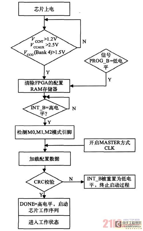
After the system or chip is powered on, the signal pin PROG_B is pulled low, and the FPGA's configuration RAM memory is cleared; similarly, the logic low level on PROG_B will reset the configuration logic and keep the FPGA in the clear configuration memory state. As long as the PROG_B pin remains low, the FPGA will continue to clear its configuration RAM memory and keep the INIT_B signal low to indicate that the configuration is being cleared.
When PROG_B is released, the FPGA will continue to keep INIT_B low until all configuration memories are cleared. The FPGA detects its mode pins M0, M1, and M2 at the rising edge of the INIT_B signal.
After the INIT_B signal goes high, configuration can begin without additional pause or wait cycles. However, the configuration process does not have to start immediately after INIT_B changes. The configuration logic starts processing data only when the synchronization word of the bit stream is loaded. After power-on to clear the configuration RAM memory, the INIT_B signal pin goes high and configuration data can be loaded: the standard bit stream first introduces the idle word FFFFFFFFh, followed by the synchronization word AA995566h, and then some configuration control information, followed by the actual bit stream data frame and the related CRC; the end of the bit stream is the CRC checksum and the startup chip enters the working state. The FPGA circuit configuration flow chart is shown in Figure 2.

5 Design of FPGA dynamic aging board
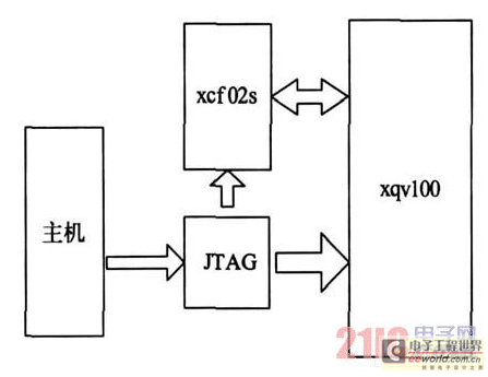
According to the configuration principle discussed above, we designed the XQV100 FPGA circuit dynamic aging board, as shown in Figure 3. The configuration mode adopts the master serial mode, which is conducive to simplifying the design of the PCB, and the configuration clock of the master serial mode comes from the inside of the FPGA, and does not need to be provided externally. In order to make the FPGA circuit work in the master serial mode, the M1, M2, and M3 pins of the circuit should be grounded. At the same time, the external configuration memory in this mode needs to use a serial data transmission memory. Here we use Xilinx's xcf02s memory, and the internal storage capacity can reach up to 2 Mbit.
The FPGA circuit dynamic aging board uses a 400mm×400mm double-layer PCB board. Decoupling and high and low frequency RC filtering are used in the design of the aging board, and current limiting measures are taken for the DC power supply and signal source. Four aging stations are designed on each aging board. In order to facilitate online debugging of the circuit, each station consists of an XCF02S, a JTAG interface, and an XQV100. The logic program for dynamic configuration of the FPGA chip is placed in the xcf02s Flash memory. The configuration program of FPGA dynamic aging is written in VHDL language, synthesized using ISE (V9.1) tools, and functionally simulated using ModelSim (V6.0). Its specific function is to divide all input and output pins into five groups, each of which realizes the 32-frequency division function, and each group is provided with a 1MHz square wave signal as input from the outside. The computer downloads the compiled configuration program to the xcf02s circuit through the Xilinx dedicated JATG download line. When the FPGA circuit is powered on, the configuration program in xcf02s is automatically downloaded to the internal RAM memory of the FPGA in a serial manner, and the FPGA runs according to the program's functions. Each circuit selects an output port with an output frequency of about 1Hz, and an LED light is connected externally as an output monitor. During the aging process, the light can be used to observe whether the circuit is working properly.

6 Results and Analysis
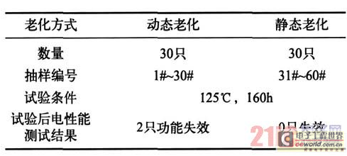
We take the XQV100 FPGA circuit as an example to conduct dynamic aging and static aging comparison tests. The test conditions are 125℃ and 160h. Randomly sample 60 circuits that pass the normal temperature test, and take 30 of each for aging according to the dynamic aging test method and the static aging test method. When the dynamic aging is powered on, ensure that each circuit has output; during the static aging test, ensure that the power supply voltage input is correct. Record once every 1h to confirm whether there is any abnormal aging.
After 26 hours, the LED of one circuit (6#) did not flash. It was initially suspected to be invalid, but it was not removed immediately. It was aged for 160 hours like other circuits. After 126 hours, the LED of 21# circuit did not flash. It continued to be tested. Within 96 hours after the aging test, the normal temperature electrical test of all circuits was completed. It was found that the functions of 6# and 21# circuits failed, and the other circuits were qualified. The specific situation is shown in Table 1.
Table 1 Comparison test results of dynamic aging and static aging

Compared with the static aging test method, the dynamic aging test is driven by the program of the peripheral configuration circuit, so that the internal functional modules of the circuit are always in a high-speed working state. On the contrary, during static aging, although there is voltage loading, there is no configuration program to drive the circuit to work, and the internal modules are always in an idle state. Therefore, the stress conditions of the FPGA circuit during dynamic aging are more severe, which is more likely to expose the potential defects of the circuit itself, thereby improving the reliability of the circuit itself.
7 Conclusion
At present, most of the aging tests for FPGA circuits in China still use static aging test methods. The characteristics are that the circuit does not work during aging, the internal gate array does not flip, and it is impossible to determine whether the circuit is abnormal during the aging process. The implementation of the FPGA circuit dynamic aging test method solves these problems, increases the output monitoring points, ensures that there are no abnormalities in the circuit aging process, and thus improves the reliability of the circuit.
This paper discusses the process and principle of FPGA circuit loading and configuration, designs a test method for FPGA circuit dynamic aging, and has been successfully implemented and applied in engineering practice.
Although the circuit and configuration process designed here are for Xilinx's Qpro Virtex Hi-Rel series XQV100 circuit, it can also be used as a reference for the dynamic configuration of other series and other companies' FPGAs. Although this method achieves the purpose of dynamic aging, it still has defects: the number of internal gates of existing FPGA circuits has exceeded 1 million gates, and general configuration programs can only occupy part of the internal resources of FPGA circuits. In addition, if more D flip-flops are used, there will be fewer shift registers, which usually results in a loss of one thing while taking care of another. Therefore, it is still difficult to achieve 100% dynamic aging test.
Previous article:High-speed FPGA PCB design technology
Next article:FPGA Implementation Method of FIR Filter
Recommended ReadingLatest update time:2024-11-17 00:08


- Popular Resources
- Popular amplifiers
-
 Analysis and Implementation of MAC Protocol for Wireless Sensor Networks (by Yang Zhijun, Xie Xianjie, and Ding Hongwei)
 -
 MATLAB and FPGA implementation of wireless communication
 -
 Intelligent computing systems (Chen Yunji, Li Ling, Li Wei, Guo Qi, Du Zidong)
 -
 Summary of non-synthesizable statements in FPGA
- Huawei's Strategic Department Director Gai Gang: The cumulative installed base of open source Euler operating system exceeds 10 million sets
- Analysis of the application of several common contact parts in high-voltage connectors of new energy vehicles
- Wiring harness durability test and contact voltage drop test method
- Sn-doped CuO nanostructure-based ethanol gas sensor for real-time drunk driving detection in vehicles
- Design considerations for automotive battery wiring harness
- Do you know all the various motors commonly used in automotive electronics?
- What are the functions of the Internet of Vehicles? What are the uses and benefits of the Internet of Vehicles?
- Power Inverter - A critical safety system for electric vehicles
- Analysis of the information security mechanism of AUTOSAR, the automotive embedded software framework
 Professor at Beihang University, dedicated to promoting microcontrollers and embedded systems for over 20 years.
- Innolux's intelligent steer-by-wire solution makes cars smarter and safer
- 8051 MCU - Parity Check
- How to efficiently balance the sensitivity of tactile sensing interfaces
- What should I do if the servo motor shakes? What causes the servo motor to shake quickly?
- 【Brushless Motor】Analysis of three-phase BLDC motor and sharing of two popular development boards
- Midea Industrial Technology's subsidiaries Clou Electronics and Hekang New Energy jointly appeared at the Munich Battery Energy Storage Exhibition and Solar Energy Exhibition
- Guoxin Sichen | Application of ferroelectric memory PB85RS2MC in power battery management, with a capacity of 2M
- Analysis of common faults of frequency converter
- In a head-on competition with Qualcomm, what kind of cockpit products has Intel come up with?
- Dalian Rongke's all-vanadium liquid flow battery energy storage equipment industrialization project has entered the sprint stage before production
- Allegro MicroSystems Introduces Advanced Magnetic and Inductive Position Sensing Solutions at Electronica 2024
- Car key in the left hand, liveness detection radar in the right hand, UWB is imperative for cars!
- After a decade of rapid development, domestic CIS has entered the market
- Aegis Dagger Battery + Thor EM-i Super Hybrid, Geely New Energy has thrown out two "king bombs"
- A brief discussion on functional safety - fault, error, and failure
- In the smart car 2.0 cycle, these core industry chains are facing major opportunities!
- The United States and Japan are developing new batteries. CATL faces challenges? How should China's new energy battery industry respond?
- Murata launches high-precision 6-axis inertial sensor for automobiles
- Ford patents pre-charge alarm to help save costs and respond to emergencies
- New real-time microcontroller system from Texas Instruments enables smarter processing in automotive and industrial applications
- 【ST NUCLEO-H743ZI Review】+ 4. Serial port output
- ZigBee Protocol Stack
- EEWORLD University ---- Fundamentals of VLSI Design (Fundamentals of Digital Integrated Circuit Design) (Southeast University)
- CH340 circuit to prevent current backflow
- Bluetooth module responds incorrectly
- 【RT-Thread Reading Notes】Reflections on RT-Thread Learning Chapter 6
- LTspice(2) .TEXT uses Xnn
- 【What should I do】Bullshit
- STM32 supports VCP+MSC+HID mode
- How does AD20 perform multi-person collaboration? (Multiple picture warning

 Analysis and Implementation of MAC Protocol for Wireless Sensor Networks (by Yang Zhijun, Xie Xianjie, and Ding Hongwei)


 京公网安备 11010802033920号