0 Introduction
LDPC code was first proposed by Gallager in 1962 and can be regarded as a linear block code with a sparse check matrix. Since Mackay and Neal found that the performance of LDPC code is very close to the Shannon limit, LDPC code has attracted more and more attention. Based on the structural characteristics of quasi-cyclic LDPC (QC-LDPC) code, a design method for QC-LDPC decoder supporting multiple code rates is proposed, and a universal QC-LDPC decoder that can adaptively support three different H matrices in real time is designed and implemented.
1 Introduction to QC-LDPC Codes
The check matrix Hqc of the QC-LDPC code is composed of c × t circulant permutation matrices, where c and t are both integers and c < t. Each permutation matrix in the check matrix of the QC-LDPC code is replaced by the corresponding shift value, thus obtaining a new matrix, called the basic matrix. The basic matrix corresponds to the H matrix one-to-one. The structure of the QC-LDPC rule makes its coding easy to implement in engineering, so many LDPC codes in the standards use QC-LDPC codes.
2. Introduction to Decoding Algorithm
The decoder designed here mainly adopts the offset value minimum sum algorithm based on soft decision. The offset value minimum sum algorithm is improved on the basis of the sum-product algorithm and the minimum sum algorithm, and has the characteristics of low decoding complexity and excellent performance. In order to better describe the algorithm, some symbols are defined first.
L(ci) represents the original soft information of variable node i of the input decoder, L(rji) represents the information transmitted from check node j to variable node i, and L(qij) represents the information transmitted from variable node i to check node j. The meanings of αij and βi'j are shown in formula 1:

The specific algorithm steps are as follows:
Initialize the original probability information of the codeword.

Step 1: Update the probability information of the check node (CNU, Check NodeUpdate).

Step 2: Update the probability information of the information node (VNU, Variable NodeUpdate).

Also calculate:

LQ makes a hard decision. If ( ) 0 i LQ > , the decision is 0, otherwise 1. Calculate whether cHT is 0 or the maximum number of iterations has been reached. If so, go to step 3, otherwise go to step 1.
Step 3: Output the judgment result.
Through simulation, the decoder input fixed-point scheme determined in this paper is as follows: the quantization bit width is 6 bits, of which 3 bits represent integer bits and 2 bits represent decimal bits.
3 Multi-rate LDPC decoder design
First, consider the following three QC-LDPC codewords as references, with a code length of 8064 bits and code rates of 7/8, 3/4, and 1/2. The optimal offset values (offset values in (3)) required by the minimum and decoding algorithms for different code rates are obtained through simulation, which are 1, 0.7, and 0.5, respectively. The code expansion factor used in the above QC-LDPC code is 112.
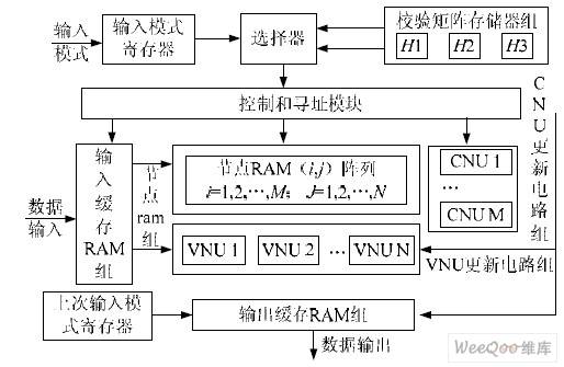
The LDPC decoder implemented in this paper is based on a partially parallel decoding structure. The decoder performs double buffering of input and output to support continuous data processing. The overall structure is shown in Figure 1.

Figure 1 Overall structure of the decoder
Since three different H-matrix LDPC codes are to be supported, a mode port is required to inform the decoder which code type the current data block belongs to. The input mode register controls the selector to select different H-matrixes to configure the control and addressing module, so that it can select the node RAM that needs to be updated and the circuit sets of the check node unit (CNU) and variable node unit (VNU) that need to be updated.
The input data is first input into the input cache RAM group, which is divided into N blocks according to the number of columns of the basic matrix to cache the data, where N is configurable and the N used in this paper is 72. After the data is full of a frame of coding blocks, it is input into the node RAM group. The role of the node RAM group is to store the intermediate information during the algorithm iteration update. Since there are more zero matrices in the basic matrix, the number of node RAMs actually generated is much smaller than M × N.
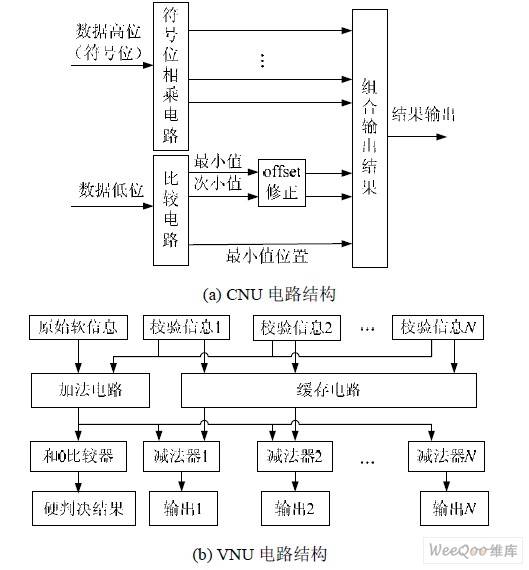
The purpose of the CNU circuit is to update the probability of the check node and complete the calculation of equation (3). The implementation structure is shown in Figure 2 (a). The purpose of the VNU circuit is to update the probability of the variable node and calculate the hard decision result at the same time to complete the calculation of equations (4) and (5).
The specific structure is shown in Figure 2(b).

Figure 2 Structure of CNU and VNU circuits
The output buffer RAM group is used to store and output the decoding results. It also adopts ping-pong operation to support continuous input and output of data blocks. The control and addressing module is the core module of the decoder. It provides various control signals and addressing signals for reading and writing RAM for the decoder. The addressing module is divided into two parts: CNU address generation module and VNU address generation module. The starting address of CNU address generation module is its offset value; while the addresses generated by VNU address are from 0 to Z.
Due to the use of input and output double buffering, there can be at most three data blocks in the decoder, and these three data blocks can be data blocks with different code rates, thus realizing the function of adaptive decoding of continuously input data blocks with different code rates.
4 FPGA implementation and performance testing:
According to the above design scheme, Verilog HDL was selected for design, Modelsim 6.1b was used for simulation verification, and finally the test was carried out on the Stratix IIEP2S180F1020I4 chip. See Table 1 for details.
Table 1 Resource usage

Table 1 also lists the resource usage of a single-rate decoder (7/8 bit rate). It can be seen that the multi-rate decoder can effectively support three bit rates under the premise that the resource usage does not exceed the sum of the resources of the decoders of two bit rates.
At the same time, the throughput and the highest operating clock of each bit rate were tested. The highest operating clock of the three bit rates (1/2, 3/4, 7/8) is 110 MHz, and the highest throughput is 110 Mb/s, 165 Mb/s and 192.5 Mb/s respectively. From the test results, it can be seen that the throughput of the multi-rate decoder is also above 110 Mb/s, indicating that it still maintains a high decoding throughput while meeting the requirements of adaptive multi-rate applications.
5 Conclusion
According to the characteristics of QC-LDPC code, a multi-rate QC-LDPC decoder implementation method is proposed, and this universal multi-rate decoder is implemented using FPGA, which can support at least three different QC-LDPC codes. The input and output parameters of this multi-rate QC-LDPC decoder can be flexibly configured according to the required supported code types, and the final decoding throughput can exceed 110 Mb/s for any code rate, taking into account the flexibility and high throughput required by the multi-rate decoder.
Previous article:Research and Implementation of 8PSK Soft Demodulation Based on FPGA
Next article:Design of Partial Response CPM Signal Demodulator Based on FPGA
- Huawei's Strategic Department Director Gai Gang: The cumulative installed base of open source Euler operating system exceeds 10 million sets
- Analysis of the application of several common contact parts in high-voltage connectors of new energy vehicles
- Wiring harness durability test and contact voltage drop test method
- Sn-doped CuO nanostructure-based ethanol gas sensor for real-time drunk driving detection in vehicles
- Design considerations for automotive battery wiring harness
- Do you know all the various motors commonly used in automotive electronics?
- What are the functions of the Internet of Vehicles? What are the uses and benefits of the Internet of Vehicles?
- Power Inverter - A critical safety system for electric vehicles
- Analysis of the information security mechanism of AUTOSAR, the automotive embedded software framework
 Professor at Beihang University, dedicated to promoting microcontrollers and embedded systems for over 20 years.
- Innolux's intelligent steer-by-wire solution makes cars smarter and safer
- 8051 MCU - Parity Check
- How to efficiently balance the sensitivity of tactile sensing interfaces
- What should I do if the servo motor shakes? What causes the servo motor to shake quickly?
- 【Brushless Motor】Analysis of three-phase BLDC motor and sharing of two popular development boards
- Midea Industrial Technology's subsidiaries Clou Electronics and Hekang New Energy jointly appeared at the Munich Battery Energy Storage Exhibition and Solar Energy Exhibition
- Guoxin Sichen | Application of ferroelectric memory PB85RS2MC in power battery management, with a capacity of 2M
- Analysis of common faults of frequency converter
- In a head-on competition with Qualcomm, what kind of cockpit products has Intel come up with?
- Dalian Rongke's all-vanadium liquid flow battery energy storage equipment industrialization project has entered the sprint stage before production
- Allegro MicroSystems Introduces Advanced Magnetic and Inductive Position Sensing Solutions at Electronica 2024
- Car key in the left hand, liveness detection radar in the right hand, UWB is imperative for cars!
- After a decade of rapid development, domestic CIS has entered the market
- Aegis Dagger Battery + Thor EM-i Super Hybrid, Geely New Energy has thrown out two "king bombs"
- A brief discussion on functional safety - fault, error, and failure
- In the smart car 2.0 cycle, these core industry chains are facing major opportunities!
- The United States and Japan are developing new batteries. CATL faces challenges? How should China's new energy battery industry respond?
- Murata launches high-precision 6-axis inertial sensor for automobiles
- Ford patents pre-charge alarm to help save costs and respond to emergencies
- New real-time microcontroller system from Texas Instruments enables smarter processing in automotive and industrial applications
- The 4th volume of Mr. Yang's new book "New Concept Analog Circuits" is online! Hurry up if you need it~
- Can UC28025 be frequency modulated?
- Modification + Disassembly of portable ion air purifier and modification of coal stove lighter 2---Modification was successful and the cause of failure was found.
- Free application for Vicor high power DC-DC converter / ZVS buck regulator
- [2022 Digi-Key Innovation Design Competition] Raspberry Pi collects power grid data
- Unlock the TE mobile micro website and get one-stop resources!
- Design an electronic meter that can measure 0-1.5A current and automatically switch ranges
- MSP430 emulator instructions and msp430f5438 minimum system circuit
- Which domestic fast-charging chip is the best?
- What does 0402_SHORT mean in the schematic diagram and how to draw the PCB

 CVPR 2023 Paper Summary: Video: Low-Level Analysis, Motion, and Tracking
 Deep Learning Made Easy: Core Algorithms and Visual Practice (Feng Chao)


 京公网安备 11010802033920号