A controllable vibrator is a seismic exploration signal excitation device. In oil exploration, it has the advantages of low construction cost, safety and environmental protection, flexible construction organization, and artificial control of the excitation signal. The application of controllable vibrators in seismic construction at home and abroad is relatively common. Except for water areas, swamps, and mountains supported by helicopters, as long as the seismic source can enter, it is required to use controllable vibrators for construction. The scanning signal generator in the controllable vibrator is located at the forefront of the system. Its performance indicators directly affect the harmonic distortion caused by power supply interference, which has a great impact on the quality and resolution of seismic data. How to improve its amplitude and frequency accuracy is the key to the design.
1 Hardware Design
1.1 Overview
The main function of the system is to realize the analog sweep frequency signal source . Its main principle is to first control the DSP chip to generate a linear digital sweep frequency signal through key interrupt or host computer interrupt , and then send this signal to the D/A chip DAC8565 for digital-to-analog conversion to output a linear analog sweep frequency signal. After signal conditioning, the output system obtains the required signal source. The hardware flow block diagram is shown in Figure 1.
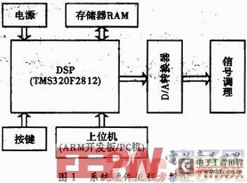
Among them, the key interrupt is realized through the interrupt of GPIO and PIE, and the host computer interrupt is realized through the interrupt of SCI module of TMS320F2812 . The digital signal generated by DSP chip TMS320F2812 is transmitted to DAC8565 of D/A conversion chip through its SPI module for digital-to-analog conversion.
1.2 TMS320F2812 minimum system
A typical DSP minimum system includes DSP chip, power supply circuit, reset circuit, clock circuit and serial communication circuit, etc.
(1) Design of power supply and reset circuit. DSP system generally adopts multi-power supply system. The design of power supply and reset circuit has an important influence on system performance. The minimum DSP system is powered by 5 V power supply. Since the power supply voltage of DSP chip is 3.3 V, it is necessary to convert 5 V power supply to 3.3 V to power CPU when designing the circuit. This paper adopts TI's TPS767D318 power supply chip. This chip is a linear step-down DC conversion chip. It can generate two different voltages of 3.3 V, 1.8 V or 2.5 V from 5 V power supply at the same time. Its maximum output current is 1000 mA, which can meet the power supply requirements of a DSP chip and a small number of peripheral circuits at the same time. The power monitoring and reset management functions of this chip also meet the system requirements.
(2) Clock circuit design. The clock of TMS320F2812 DSP can be connected internally or externally. If the internal oscillator is used, a quartz crystal must be connected between the two pins X1/XCLKIN and X2. If an external clock is used, the input clock signal can be directly connected to X1/CI.
On the KIN pin, X2 is left floating. This article uses an external active clock mode, using a 3.3 V powered 30 MHz active crystal oscillator, and programming to achieve the maximum operating frequency of F2812 150 MHz.
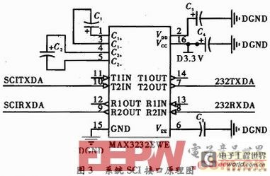
(3) DSP serial interface design. The TTL level of the SCI interface in TMS320F2812 is incompatible with the RS-232C level of the PC, which requires that level conversion must be considered when designing the interface. The design uses the MAX232N driver chip for serial communication, which complies with the RS-232 standard, has low power consumption, high integration, +5 V power supply, two receiving and transmitting channels, and matches the two SCI interfaces of TMS320 F2812.
1.3 Key Interrupt
As shown in Figure 2, the system interruption part has 4 buttons, namely S1, S2, S3, and S4, whose functions are start frequency sweep output/stop frequency sweep output, start sweep frequency setting/stop sweep frequency setting, frequency increase, and frequency decrease. The system starts frequency sweep output when S1 is pressed for the first time, and the system stops frequency sweep output when S1 is pressed for the second time. The system starts frequency sweep setting when S2 is pressed for the first time, and stops frequency sweep setting when S2 is pressed for the second time. Each time S3 is pressed, the sweep frequency increases by a certain value. Similarly, each time S4 is pressed, the sweep frequency decreases by a certain value.
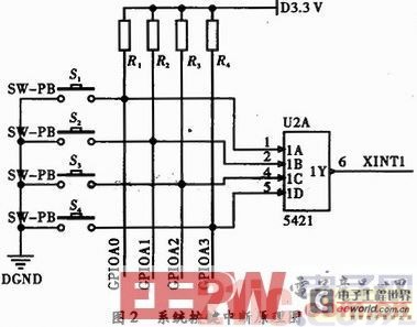
Whenever a key is pressed, XINT1 will have a level jump, which will be read by the TMS320F2812 chip, the GPIO port will be started to read the key information, and the relevant judgment program will be used to determine which key is pressed, and then the function implementation program of the corresponding key will be entered to complete the key interrupt.
1.4 Host computer interrupt
In addition to using key interrupts to control the frequency sweep signal source, the system can also be controlled by the host computer connected to the SCI port of the DSP chip TMS320F2812. The relevant interface principle is shown in Figure 3.
1.5 Interface Design
The linear digital frequency sweep signal generated by TMS320F2812 must be converted from digital to analog before it can be converted into a linear analog frequency sweep signal. The chip used in the design of the D/A converter is DAC8565, which is a low-power, 4-channel, 16-bit precision voltage output digital-to-analog converter. The device integrates an internal reference power supply of 2.5 V, 2 ppm/℃, and also integrates a serial SPI communication port with a clock rate of up to 50 MHz.
The system uses the digital frequency sweep signal generated by TMS320F2812 to transmit to the digital signal input port of DAC8565 through the SPI interface, and then outputs the analog signal through digital-to-analog conversion, and the signal conditioning channel outputs the required analog frequency sweep signal.
2 Software Design
2.1 Principle of Linear Sweep Signal
In theory, the frequency of a linear sweep signal changes linearly with time, which can be expressed as

Where F1 is the start frequency of the scan; F2 is the end frequency of the scan; and T is the duration of the scan. The START TAPER and END TAPER periods are not considered in this expression.
In practical applications, a TAPER segment is necessary. Its mathematical expression is:

Where TD is the sweep length; T1 is the start sweep time window length.
2.2 Key Interrupt
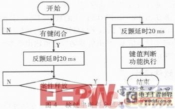
The key interruption part judges whether there is a level jump on the XINT1 port through its response program to ensure whether a key is pressed. If a key is pressed, the corresponding key function implementation program in the TMS320F2812 chip will be started to implement the function of the corresponding key and complete the key interruption. The process is shown in Figure 4.
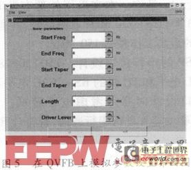
The interrupt part of the host computer can realize interrupt control through SCI port communication with the chip through the ARM development board or PC. When the host computer is a PC, the host computer control interface shown in Figure 5 can be constructed through software programming. And the work of the sweep signal source can be controlled by performing corresponding operations on the interface through the mouse and keyboard .
2.4 Digital-to-analog conversion part
This part is an important part of the system. Its function is to convert the digital frequency sweep signal generated by the front end of the system into digital-to-analog signals and perform signal conditioning to output the analog frequency sweep signal required by the system. The digital frequency sweep signal generated by TMS320F2812 is output through its SPI port and transmitted to the digital signal input port of the digital-to-analog conversion chip DAC8565. After digital-to-analog conversion in DAC8565, the analog frequency sweep signal is obtained. Then, it is amplitude-scaled and filtered through the conditioning channel to make its output amplitude within the required range, and the deformed part of its waveform signal is greatly reduced, so that the waveform distortion is smaller. The main process is shown in Figure 6.

3 System Simulation
Set the starting frequency to 6 Hz, the ending frequency to 80 Hz, and the time window to 0.5 s. The simulation results are as follows.
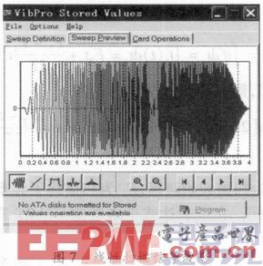
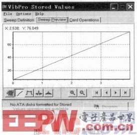
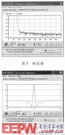
It can be seen from the above figure that the linear frequency sweep signal generated by the above method has good frequency output linearity, high precision, stable waveform, small distortion and strong anti-interference ability. In addition, the operation of the frequency sweep signal generator is convenient and the operation is relatively stable, which meets the requirements of engineering applications.
4 Conclusion
This paper proposes a solution for implementing a linear frequency sweep signal generator based on a DSP platform, introduces the design principle in detail, and discusses the key contents that need to be completed in the design process. The fast computing speed of DSP is used to generate linear frequency sweep signals in real time. The system uses the DSP chip model TMS320F2812 as the computing processing and interrupt response chip to generate digital frequency sweep signals, and uses the D/A converter DAC8565 for digital-to-analog conversion, and then outputs analog frequency sweep signals after signal conditioning. The development prospects of this new frequency sweep signal generator are broad.
Previous article:Design of video processing system based on FPGA+DSP architecture
Next article:Design of serial communication system based on DSP and touch screen
Recommended ReadingLatest update time:2024-11-16 14:49


- Popular Resources
- Popular amplifiers
- Huawei's Strategic Department Director Gai Gang: The cumulative installed base of open source Euler operating system exceeds 10 million sets
- Analysis of the application of several common contact parts in high-voltage connectors of new energy vehicles
- Wiring harness durability test and contact voltage drop test method
- Sn-doped CuO nanostructure-based ethanol gas sensor for real-time drunk driving detection in vehicles
- Design considerations for automotive battery wiring harness
- Do you know all the various motors commonly used in automotive electronics?
- What are the functions of the Internet of Vehicles? What are the uses and benefits of the Internet of Vehicles?
- Power Inverter - A critical safety system for electric vehicles
- Analysis of the information security mechanism of AUTOSAR, the automotive embedded software framework
 Professor at Beihang University, dedicated to promoting microcontrollers and embedded systems for over 20 years.
- Innolux's intelligent steer-by-wire solution makes cars smarter and safer
- 8051 MCU - Parity Check
- How to efficiently balance the sensitivity of tactile sensing interfaces
- What should I do if the servo motor shakes? What causes the servo motor to shake quickly?
- 【Brushless Motor】Analysis of three-phase BLDC motor and sharing of two popular development boards
- Midea Industrial Technology's subsidiaries Clou Electronics and Hekang New Energy jointly appeared at the Munich Battery Energy Storage Exhibition and Solar Energy Exhibition
- Guoxin Sichen | Application of ferroelectric memory PB85RS2MC in power battery management, with a capacity of 2M
- Analysis of common faults of frequency converter
- In a head-on competition with Qualcomm, what kind of cockpit products has Intel come up with?
- Dalian Rongke's all-vanadium liquid flow battery energy storage equipment industrialization project has entered the sprint stage before production
- Allegro MicroSystems Introduces Advanced Magnetic and Inductive Position Sensing Solutions at Electronica 2024
- Car key in the left hand, liveness detection radar in the right hand, UWB is imperative for cars!
- After a decade of rapid development, domestic CIS has entered the market
- Aegis Dagger Battery + Thor EM-i Super Hybrid, Geely New Energy has thrown out two "king bombs"
- A brief discussion on functional safety - fault, error, and failure
- In the smart car 2.0 cycle, these core industry chains are facing major opportunities!
- The United States and Japan are developing new batteries. CATL faces challenges? How should China's new energy battery industry respond?
- Murata launches high-precision 6-axis inertial sensor for automobiles
- Ford patents pre-charge alarm to help save costs and respond to emergencies
- New real-time microcontroller system from Texas Instruments enables smarter processing in automotive and industrial applications
- TouchGFX Design + HMI Design for HVAC Air Conditioning
- [Repost] 10 rules for PCB layout and wiring
- Switching Power Supply
- Dual-core communication exchanges data through shared memory ARM-side program learning
- Please recommend a newer rf development kit
- Triangle wave generating circuit
- [RT-Thread Reading Notes] Part 2 (1) Porting, Running and Thread Management
- Are you confused about gate driver selection? Download the latest selection guide
- Wish you all a happy Dragon Boat Festival
- Using MCU to implement speech recognition? MSP432 can do it!

 MATLAB and FPGA implementation of wireless communication


 京公网安备 11010802033920号