The traditional digital phase-locked loop design hopes to obtain stable oscillation control data by adopting a loop filter with low-pass characteristics in structure. However, in the digital phase-locked loop system based on digital logic circuit design, it is difficult to implement low-pass filtering using logic algorithms. Therefore, some pulse train low-pass filter counting circuits have emerged, among which the most common is the "N before M" loop filter. These circuits obtain the oscillation control parameters of the controllable oscillator module by counting the phase error pulses generated by the phase detection module. The pulse train low-pass filter counting method is a relatively complex nonlinear processing process, which is difficult to linearly approximate, so it is impossible to use the system transfer function analysis method to determine the design parameters in the phase-locked loop and further analyze the phase-locked performance. In terms of design methods, VHDL language or Verilog HDL language programming is often used to complete the system design, and EDA software is used to perform timing simulation on the system to verify the correctness of the design. This design method requires the designer to have a certain understanding of FPGA hardware and a solid foundation in hardware description language programming.
This paper adopts a loop filter based on proportional integral (PI) control algorithm to apply to the bandwidth adaptive all-digital phase-locked loop, establishes the mathematical model of the phase-locked loop, and analyzes the relationship between the various performance indicators and design parameters of the phase-locked loop. The obtained mathematical model of the phase-locked loop is directly modeled at the system level in the Matlab/Simulink environment using DSP Builder, and computer simulation is performed. At the same time, the established model file is converted into VHDL program code, simulated and verified in QuartusⅡ software, and implemented with FPGA.
1 Theoretical Analysis of Bandwidth Adaptive All-Digital Phase-Locked Loop
1.1 Theoretical Analysis of Analog Phase-Locked Loop Based on PI Control
The phase-locked loop is a negative feedback system, which mainly consists of three parts: phase detector (PD), loop filter (LF) and voltage-controlled oscillator (VCO). The function of the phase detector is to calculate the phase error between the input signal and the output signal. The main function of the loop filter is to suppress noise and high-frequency components, and control the speed and accuracy of the loop phase correction. In order to improve the performance of the phase-locked system, this paper adopts a first-order low-pass filter based on the PI control algorithm, that is, the phase error identified by the phase detector module is multiplied by a certain proportional coefficient to generate a proportional control parameter, and the phase error is integrated at the same time, and an integral control parameter is generated under the adjustment of the integral coefficient. Finally, the sum of the proportional and integral control parameters is taken as the control parameter of this link. The function of the voltage-controlled oscillator is to use the input voltage value to control the frequency of the output signal. Assume that the input signal of the voltage-controlled oscillator is V0(t), and the frequency of the output signal is ω0+KV0(t), then the phase of the output signal is:
![]()
Where: ![]() , then the transfer function of the voltage-controlled oscillator is: HVCO(s)=θf(s)/V0(t)=K/s, it can be seen that the voltage-controlled oscillator is equivalent to an inherent integral link. In this design, the gain of the voltage-controlled oscillator K=1, then through the above analysis, the block diagram of the analog phase-locked loop based on the PI control algorithm can be obtained as shown in Figure 1.
, then the transfer function of the voltage-controlled oscillator is: HVCO(s)=θf(s)/V0(t)=K/s, it can be seen that the voltage-controlled oscillator is equivalent to an inherent integral link. In this design, the gain of the voltage-controlled oscillator K=1, then through the above analysis, the block diagram of the analog phase-locked loop based on the PI control algorithm can be obtained as shown in Figure 1. 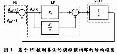
It can be concluded from Figure 1 that the closed-loop transfer function of the phase-locked loop is:
![]()
It is not difficult to see that this system is a typical second-order system, then the closed-loop transfer function of the second-order analog phase-locked loop can be expressed as:

Where: Kp and Kl are the proportional coefficient and integral coefficient respectively, taken ![]() as the natural frequency of the system; ζ is the damping coefficient of the system.
as the natural frequency of the system; ζ is the damping coefficient of the system.
1.2 Theoretical Analysis of Bandwidth Adaptive All-Digital Phase-Locked Loop
The s-domain transfer function of the above analog phase-locked loop is discretized, and the closed-loop transfer function of the full digital phase-locked loop can be obtained by using the impulse response invariance method:
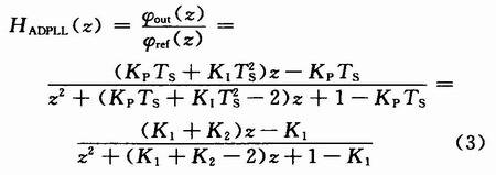

Therefore, the structure diagram of the fully digital phase-locked loop based on parameters K1 and K2 can be obtained as shown in FIG2 .
Analyze the two parameters K1 and K2 obtained in formula (5). If c and ζ are constants, the changes of parameters K1 and K2 are only related to the changes of the input signal frequency ωref. Therefore, the obtained full digital phase-locked loop model has adaptive characteristics, which is a new feature that the traditional full digital phase-locked loop does not have.
2 DSP Builder Modeling of Bandwidth Adaptive All-Digital Phase-Locked Loop
2.1 Introduction to DSP Builder
Due to the widespread application of FPGA, EDA software QuartusⅡ is particularly important in many fields. At present, the design of full digital phase-locked loop is mostly completed through EDA technology and implemented using FPGA. This requires designers to be very familiar with FPGA hardware circuits and hardware description languages VHDL or Verilog HDL; at the same time, it is quite cumbersome to use hardware description languages to program and design system modules in the QuartusⅡ environment. Matlab is powerful in building mathematical models of the system, and has a special modeling and simulation tool Simulink, which can perform graphical modeling and simulation. However, Matlab itself does not support hardware circuits and can only complete the modeling and simulation of simple mathematical models. If the advantages of the two are combined and the strengths of the two are used to avoid weaknesses, the design of complex electronic systems can become quite easy and intuitive.
DSP Builder is a system tool for DSP development launched by Altera. It is a Simulink toolbox for Matlab, and can be used for graphical modeling and simulation in the atlab/Simulink environment. The modules in DSP Builder are described at the algorithm level, which makes it easy for users to model at the system or algorithm level, and they don't even need to fully understand FPGA itself and hardware description language. The module library of DSPBuilder also provides the interface module Signal Compiler for Matlab and QuartusⅡ. This module can be used to easily convert the algorithm or system-level model established in the Matlab/Simulink environment into a VHDL language program with the suffix .vhd that can be compiled by FPGA. Open the project file in QuartusⅡ, and you can compile and simulate the generated program. After completion, you can lock the pins according to the pin situation of the FPGA development board. After compilation and adaptation, it can be downloaded to the FPGA development board to complete hardware testing and hardware implementation.
2.2 DSP Builder Modeling of Bandwidth Adaptive All-Digital Phase-Locked Loop
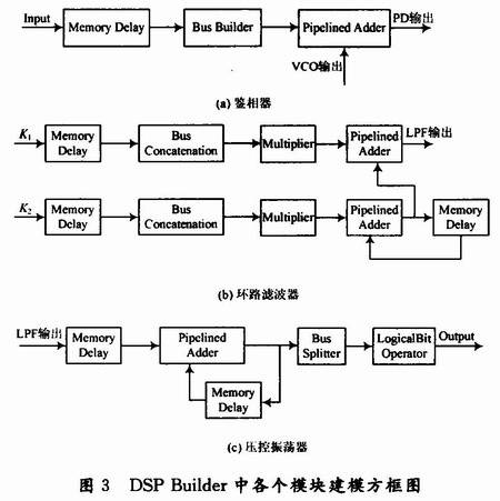
The design method is to use DSP Builder in Matlab/Simulink environment to simply, conveniently and quickly establish the mathematical model of the all-digital phase-locked loop obtained by the above analysis. The modeling block diagram of each module is shown in Figure 3. According to the above block diagrams, the entire system model is connected, and the system clock Clock module and Signal Compiler module are added to complete the DSP Builder modeling of the entire system. The input signals K1 and K2 are calculated by formula (5) and represented by 6-bit unsigned integers. K1 and K2 can be adjusted adaptively with the change of the input signal Phi_ref frequency; Phi_ref and Phi_out are the input and output signals of the loop respectively, and both are represented by 1-bit unsigned integers.
3 Software Simulation and FPGA Implementation of Bandwidth Adaptive All-Digital Phase-Locked Loop
3.1 Software Simulation of Bandwidth Adaptive All-Digital Phase-Locked Loop
Based on the model established in Figure 3, the design first performs software simulation on the bandwidth adaptive all-digital phase-locked loop, mainly including Matlab/Simulink simulation and QuartusⅡ timing simulation. The system parameters are: damping coefficient ζ = 0.707, system clock period Tclk = 1/fs, sampling frequency fs = 250 MHz. Figure 4 shows the Matlab/Simulink simulation waveform when the input signal Phi_ref takes different frequencies.
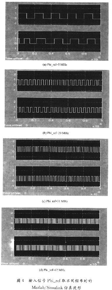
The Signal Compiler module in the DSP Builder library is used to convert the fully digital phase-locked loop model established in Figure 3 into VHDL language code. The design uses QuartusⅡ software to complete the overall timing simulation of the bandwidth adaptive fully digital phase-locked loop. Figure 5 is the timing simulation diagram when the input signal Phi_ref jumps from 20 MHz to 5 MHz; Figure 6 is the timing simulation diagram when the input signal Phi_ref jumps from 31 MHz to 62 MHz. Through the Matlab/Simu-link simulation and QuartusⅡ timing simulation of the designed fully digital phase-locked loop, it can be seen that the system can realize the frequency locking function; at the same time, the system has adaptive characteristics and has good performance in a large range of input signal changes; finally, the system also has good tracking performance for input signals with step jumps in frequency.

3.2 FPGA Implementation and Hardware Testing
Since the Signal Compiler module can automatically convert the model file created by DSPbuilder into the project file under the QuartusⅡ environment, the design is combined with the FPGA test box after completing the software simulation, and the pins are locked, compiled and adapted to be downloaded to the FPGA chip under the generated project to realize the designed bandwidth adaptive full digital phase-locked loop and complete the hardware test. Signal generators and oscilloscopes are required in hardware testing. The signal generator is used to generate the input test signal of the phase-locked loop, and the oscilloscope is used to observe the input/output waveform of the phase-locked loop. Figure 7 shows the measured waveforms when the input signal Phi_ref takes different frequencies.
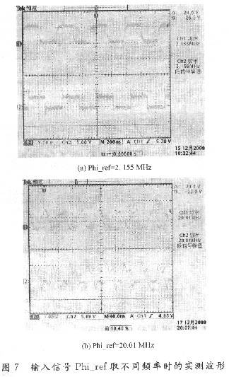
The above software simulation and hardware tests show that the designed bandwidth adaptive all-digital phase-locked loop system can realize the frequency locking function, and the design is successful and feasible
.
This paper uses DSP Builder to build a system model to complete the design of a fully digital phase-locked loop, and the theoretical analysis and simulation results are basically consistent. From the above design process, it can be seen that the method of completing the design of a fully digital phase-locked loop based on DSP Builder allows designers to use Simulink's fast and flexible modeling and simulation functions and Matlab's powerful data analysis capabilities to perform FPGA system-level modeling and simulation, and frees designers from the tedious work of writing code languages such as VHDL or Verilog HDL, and focuses on building system models under Matlab/Simulink, shortening the design cycle and improving design flexibility.
Previous article:Design and Implementation of Polyphase Filter Based on Mid-range FPGA
Next article:DSP Performance Analysis of FPGAs
Recommended ReadingLatest update time:2024-11-16 14:41


- Popular Resources
- Popular amplifiers
- Huawei's Strategic Department Director Gai Gang: The cumulative installed base of open source Euler operating system exceeds 10 million sets
- Analysis of the application of several common contact parts in high-voltage connectors of new energy vehicles
- Wiring harness durability test and contact voltage drop test method
- Sn-doped CuO nanostructure-based ethanol gas sensor for real-time drunk driving detection in vehicles
- Design considerations for automotive battery wiring harness
- Do you know all the various motors commonly used in automotive electronics?
- What are the functions of the Internet of Vehicles? What are the uses and benefits of the Internet of Vehicles?
- Power Inverter - A critical safety system for electric vehicles
- Analysis of the information security mechanism of AUTOSAR, the automotive embedded software framework
 Professor at Beihang University, dedicated to promoting microcontrollers and embedded systems for over 20 years.
- Innolux's intelligent steer-by-wire solution makes cars smarter and safer
- 8051 MCU - Parity Check
- How to efficiently balance the sensitivity of tactile sensing interfaces
- What should I do if the servo motor shakes? What causes the servo motor to shake quickly?
- 【Brushless Motor】Analysis of three-phase BLDC motor and sharing of two popular development boards
- Midea Industrial Technology's subsidiaries Clou Electronics and Hekang New Energy jointly appeared at the Munich Battery Energy Storage Exhibition and Solar Energy Exhibition
- Guoxin Sichen | Application of ferroelectric memory PB85RS2MC in power battery management, with a capacity of 2M
- Analysis of common faults of frequency converter
- In a head-on competition with Qualcomm, what kind of cockpit products has Intel come up with?
- Dalian Rongke's all-vanadium liquid flow battery energy storage equipment industrialization project has entered the sprint stage before production
- Allegro MicroSystems Introduces Advanced Magnetic and Inductive Position Sensing Solutions at Electronica 2024
- Car key in the left hand, liveness detection radar in the right hand, UWB is imperative for cars!
- After a decade of rapid development, domestic CIS has entered the market
- Aegis Dagger Battery + Thor EM-i Super Hybrid, Geely New Energy has thrown out two "king bombs"
- A brief discussion on functional safety - fault, error, and failure
- In the smart car 2.0 cycle, these core industry chains are facing major opportunities!
- The United States and Japan are developing new batteries. CATL faces challenges? How should China's new energy battery industry respond?
- Murata launches high-precision 6-axis inertial sensor for automobiles
- Ford patents pre-charge alarm to help save costs and respond to emergencies
- New real-time microcontroller system from Texas Instruments enables smarter processing in automotive and industrial applications
- MSP430 Main Memory Bootloader Introduction
- I want to use POE to power some gadgets, but I don’t know what power chip to use?
- STM8L152 drives LCD experimental ultra-low power consumption code 7.2UA
- 5G and IoT will be the great equalizer
- 【XMC4800 Relax EtherCAT Kit Review】+ Getting started with DAVE and lighting up the LED
- R4 is clearly 130 ohms, but why is it 412.147M when simulated?
- Download the Power Path Protection course materials to make future designs more reliable
- EEWORLD University ---- Industrial Motor Driver - Introduction to Texas Instruments System Solutions
- Updated PYBCN_V2 and PYBNANO_V2 firmware
- IIR filter software implementation (Matlab+C++)

 MATLAB and FPGA implementation of wireless communication


 京公网安备 11010802033920号