Motion control technology is the key foundation of manufacturing automation, and its level is an important indicator of a country's industrial modernization. Researching and developing motion controllers with open structures is an important development direction in the current motion control field. With the continuous development of integrated circuit technology, microelectronics technology, computer technology and network technology, motion controllers have evolved from motion controllers with single-chip microcomputers and microprocessors as the core and motion controllers with application-specific chips (ASICs) as the core processors to open motion controllers with co-processing architecture based on PC platforms with digital signal processors (DSPs) and field programmable gate arrays (FPGAs) as the core processors. This controller combines the information processing capabilities of PCs and DSPs with the peripheral expansion functions of FPGAs, and has the advantages of strong information processing capabilities, modularization, high degree of openness, and precise motion trajectory control.
1 System Overview
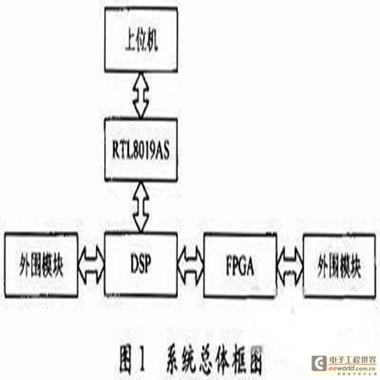
The four-axis motion controller system is based on TI's C2000 series DSP chip TMS320F2812 and alterA's CycloneⅡ series FPGA chip EP2C8F256C6. The DSP receives the control parameters of the host computer through the network port to complete the system position, speed control and motion trajectory planning; the FPGA completes the precise interpolation function of the motion controller and the expansion of the peripheral circuit. The overall block diagram of the system is shown in Figure 1. 
The main functions of the motion controller include: 4 analog voltage outputs with a voltage range of -10~+10V and a resolution of 16b; 4 pulse signal outputs; 4 pulse direction signal outputs; 4 drive reset signal outputs; 4 drive enable signal outputs; 4 differential encoding signal inputs; 4 drive alarm signal inputs; 8 positive and negative limit signal inputs; 4 origin signal inputs; 16 general digital quantities. I/O.
2DSP module design
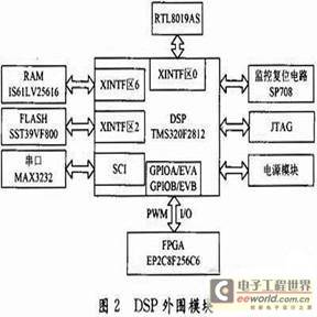
DSP calculates the planned position and planned speed in real time according to the motion mode and motion parameters received from the host computer, generates the required speed curve, and outputs the planned position in real time. TMS320F2812 is a 32-bit fixed-point DSP chip launched by TI specifically for motor control. It adopts high-performance static CMOS technology, with a main frequency of up to 150MHz (instruction cycle 6.67ns), low power consumption, core voltage of 1.8V, I/O voltage of 3.3V, supports JTAG boundary scan, and 128K×16b on-chip FLASH. There are two event managers (EVA and EVB), both of which are specific peripherals designed for multi-axis motion controllers. The external memory can be expanded through the external memory interface XINTF. The design of DSP peripheral modules is shown in Figure 2.
To enhance the anti-interference performance, DSP is connected to the host computer through the Ethernet controller RTL8019AS. RTL8019AS contains a 16KB SDRAM. DSP reads and writes it through the external memory interface to receive commands from the host computer or transmit feedback signals to the host computer. In the process of data processing, a large amount of storage space is occupied. The DSP only contains 18K×16b SARAM and 128K×16b FLASH. The storage space is too small, so 256K×16b RAM and 512K×16b FLASH are expanded through the external interface. The RAM and FLASH chips are IS61LV25616AL and SST39VF800 respectively. They have the advantages of simple interface and fast reading and writing speed. The SCI module is used to expand the RS232 serial communication interface, and the serial port chip uses MAX3232.
The voltages required by the motion controller are 5V, 3.3V, 1.8V, and 1.2V. The input voltage is 5V, and the voltage regulator chips LM1085IS3.3 and LM1117-1.8 are used to convert it into 3.3V and 1.8V respectively. Since the I/O voltage 3.3V of TMS320F2812 must be powered on before the core power supply, 1.8V must be stepped down from 3.3V to ensure the power-on sequence. 1.2V is the voltage required by the FPGA core, which is stabilized by the voltage regulator chip LM317S. The output voltage range of LM317S is 1.2~25V. The reset circuit uses the SP708 low-power microprocessor monitoring device. This device has many components, which effectively enhances the reliability and work efficiency of the system.
3FPGA module design
FPGA is used to expand axis resources. After receiving the planned position in DSP, it is transformed in the axis resource and output to the servo controller. The servo controller compares the planned position with the count position of the encoder feedback to obtain the following error, and obtains the real-time control quantity through the servo control algorithm. The control quantity is passed to the D/A converter, which converts it into a control voltage output.
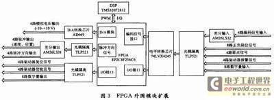
EP2C8F256C6 is a CycloneⅡ series chip from alterA. It features high performance and low power consumption, a core power supply voltage of 1.2V, 8256 logic units (LEs), 182 user I/O ports (157 I/O ports are used in the project), 165888b of internal RAM, and an embedded 18b multiplier. Each multiplier can be split into two 9b multipliers. The chip contains two phase-locked loops (PLLs) and 8 global clocks (GlobalClocks). The number of logic units, frequency, and user I/O ports of this chip can well meet the design requirements. The peripheral module expansion of FPGA is shown in Figure 3. 
3.1 Interface design with DSP
The event manager (EVA, EVB) of the DSP chip is used to connect to the FPGA. When outputting pulse quantity to control the driver, the DSP uses two event managers to control the PWM wave. When outputting analog quantity, the DSP uses GPIOA/GPIOB to output the planned position to the FPGA.
3.2 Analog signal output circuit design
The D/A converter AD669 is used to output analog signals. AD669 has two-level latches. In the design, the first-level latch of its four-way D/A chip is in a transparent state, and the second-level latch control signal LDAC is connected together. When the data of the four-way D/A chip is pre-installed, the second-level latch is opened, and the four-way D/A chips can be converted at the same time, realizing the simultaneous control of the four-axis drive.
3.3 Pulse signal output circuit design
The pulse output circuit is completed by the fine interpolator inside the FPGA. The fine interpolator generates uniform pulse output according to the coarse interpolation data sent by the DSP. The pulse output has two formats: "pulse + direction" and "positive and negative pulse". Since the differential signal has good anti-interference to external electromagnetic signals, especially the common mode interference, the pulse is isolated by the optical coupler and then connected to the differential line driver AM26LS31 for output. The function of the differential line driver AM26LS31 is to convert the input unipolar square wave signal into a pair of motor drive signals with opposite polarity.
3.4 Encoding feedback circuit design
The motor encoding signal is directly transmitted to the motor driver, and the motor driver transmits three pairs of differential encoding signals A+, A-, B+, B-, N+, N- as feedback to the motion controller. When the motor rotates, the encoded signal will have a lot of glitches, and will be interfered by the large power supply of the driver. If it is directly connected to the FPGA, it may cause misjudgment. Therefore, the three pairs of encoding signals are first converted into single-channel signals A, B, N through the differential chip AM26LS32 and then connected to the FPGA. The function of the chip AM26LS32 is to convert a pair of input encoder differential signals with opposite polarity into a unipolar pulse signal, which is exactly the opposite of AM32LS31.
3.5 Switching interface and general I/O circuit design
The output signals include reset signals and enable signals, which are generated by FPGA and directly output after optical coupling isolation; the input signals include drive alarm signals, positive and negative limit signals and origin signals, which are received by FPGA after optical coupling isolation and level conversion. When FPGA detects these signals, it determines the specific trigger signal and responds accordingly. In addition, the motion controller also provides eight digital input channels and eight digital output channels. The input and output channels are optically isolated to improve anti-interference.
4 Network port module design
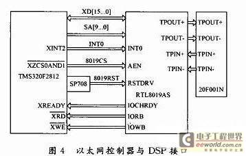
DSP is connected to the host computer through the Ethernet controller RTL8019AS. RTL8019AS integrates the RTL8019AS kernel and a 16KB SDRAM memory on a chip. It is compatible with RTL8019AS control software and NE20008b or 16b transmission. Its interface complies with Ethernet2 and IEEE802.3 standards. There are three interface modes between RTL8019AS and the host: jumper mode, PnP mode, and RT mode. This motion controller uses the jumper mode that is convenient for DSP application. The connection between DSP and RTL8019AS is shown in Figure 4. 
(1) Data bus and address bus. The data bus of RTL8019AS and the 16-bit data bus of DSP can be directly connected. The NE2000 registers in the RTL8019AS chip are accessed through the mapped I/O ports. There are 32 I/O ports in total, with address offsets from 00H to 1FH. If the I/O base address is set to 300H, the corresponding I/O port addressing range is: 300H to 31FH. Only 10 address lines are needed to address the I/O ports. Connect SA10 to SA19 to low level, and connect SA0 to SA9 according to Table 1.
As can be seen from Table 1, only 5 address lines are needed to address a 32-bit I/O port, so SA9 and SA8 can be directly connected to high level, SA5~SA7 can be connected to low level, and SA0~SA4 can be connected to the DSP's lower 5-bit address lines XA0~XA4. 
(2) Control bus. The RTL8019AS chip select signal AEN uses the DSP's extended chip select signal, IORB and IOWB are directly connected to the DSP's read and write control signals
, the interrupt output pin INT0 is connected to the DSP's XINT2, and the high-level effective reset input pin is connected to the RST of the monitoring circuit chip SP708. When the DSP is reset, the RTL8019AS is also reset.
(3) RTL8019AS and network media interface. RTL8019AS can use coaxial cable or twisted pair as the transmission medium, ground its AUI interface or leave it suspended, and use the BNC interface. The BNC interface supports 8-wire twisted pair or coaxial cable. 20F001N is a twisted pair driver, which is a coupled isolation transformer module. It can remove high-order harmonics caused by the digital characteristics of the circuit. The connection between RTL8019AS and 20F001N is shown in Figure 4. Its differential input signal TPIN+, TPIN- and differential output signal TPOUT+, TPOUT- are connected to the corresponding pins of 20F001 respectively.
5 Conclusion
On the PC platform, the data processing capabilities of DSP and the hardware characteristics of FPGA are fully utilized, so that the system can perform complex trajectory planning and high-speed interpolation while ensuring the stability and accuracy of the motion controller. This motion controller can be applied to CNC systems, robot manufacturing and other control fields.
Previous article:Design of motion controller based on DSP/FPGA Ethernet controller
Next article:Design of 1553B Aircraft Bus System Communication Software Based on FPGA/DSP Technology
Recommended ReadingLatest update time:2024-11-16 14:47


- Popular Resources
- Popular amplifiers
-
 Analysis and Implementation of MAC Protocol for Wireless Sensor Networks (by Yang Zhijun, Xie Xianjie, and Ding Hongwei)
 -
 MATLAB and FPGA implementation of wireless communication
 -
 Intelligent computing systems (Chen Yunji, Li Ling, Li Wei, Guo Qi, Du Zidong)
 -
 Summary of non-synthesizable statements in FPGA
- Huawei's Strategic Department Director Gai Gang: The cumulative installed base of open source Euler operating system exceeds 10 million sets
- Analysis of the application of several common contact parts in high-voltage connectors of new energy vehicles
- Wiring harness durability test and contact voltage drop test method
- Sn-doped CuO nanostructure-based ethanol gas sensor for real-time drunk driving detection in vehicles
- Design considerations for automotive battery wiring harness
- Do you know all the various motors commonly used in automotive electronics?
- What are the functions of the Internet of Vehicles? What are the uses and benefits of the Internet of Vehicles?
- Power Inverter - A critical safety system for electric vehicles
- Analysis of the information security mechanism of AUTOSAR, the automotive embedded software framework
 Professor at Beihang University, dedicated to promoting microcontrollers and embedded systems for over 20 years.
- Innolux's intelligent steer-by-wire solution makes cars smarter and safer
- 8051 MCU - Parity Check
- How to efficiently balance the sensitivity of tactile sensing interfaces
- What should I do if the servo motor shakes? What causes the servo motor to shake quickly?
- 【Brushless Motor】Analysis of three-phase BLDC motor and sharing of two popular development boards
- Midea Industrial Technology's subsidiaries Clou Electronics and Hekang New Energy jointly appeared at the Munich Battery Energy Storage Exhibition and Solar Energy Exhibition
- Guoxin Sichen | Application of ferroelectric memory PB85RS2MC in power battery management, with a capacity of 2M
- Analysis of common faults of frequency converter
- In a head-on competition with Qualcomm, what kind of cockpit products has Intel come up with?
- Dalian Rongke's all-vanadium liquid flow battery energy storage equipment industrialization project has entered the sprint stage before production
- Allegro MicroSystems Introduces Advanced Magnetic and Inductive Position Sensing Solutions at Electronica 2024
- Car key in the left hand, liveness detection radar in the right hand, UWB is imperative for cars!
- After a decade of rapid development, domestic CIS has entered the market
- Aegis Dagger Battery + Thor EM-i Super Hybrid, Geely New Energy has thrown out two "king bombs"
- A brief discussion on functional safety - fault, error, and failure
- In the smart car 2.0 cycle, these core industry chains are facing major opportunities!
- The United States and Japan are developing new batteries. CATL faces challenges? How should China's new energy battery industry respond?
- Murata launches high-precision 6-axis inertial sensor for automobiles
- Ford patents pre-charge alarm to help save costs and respond to emergencies
- New real-time microcontroller system from Texas Instruments enables smarter processing in automotive and industrial applications
- Internal structure of ESP8266 chip
- EEWORLD University ---- Tektronix uses mixed signal oscilloscope to explore the secrets of the bus
- Why choose 120Ω? The terminal resistance value recommended by the CAN standard
- Is there any sensor expert?
- About New Energy Vehicle Mode 2 IC-CPD Charging Gun Type A Leakage Current Sensor
- Help! What brand are the 2 UV sensors in the picture?
- Please tell me the pin definition of EPM7128S 100 pin. . . .
- BQ25120 Battery Management IC Problem Solving Sharing
- Difference between LOG_printf() and printf() in DSP
- What is the principle of this circuit?

 Analysis and Implementation of MAC Protocol for Wireless Sensor Networks (by Yang Zhijun, Xie Xianjie, and Ding Hongwei)


 京公网安备 11010802033920号