For years, digital signal processor (DSP) designers have faced a difficult task: delivering high-performance chips in a small footprint without sacrificing flexibility and software programmability.
As new applications develop at an incredible rate, the DSPs provided must keep up with this speed in terms of power, performance and longevity, meet the challenges of today and be ready for the applications of tomorrow. These high-performance multi-core DSPs are increasingly being used in telecommunications access, improved data rates for GSM services (EDGE) and infrastructure equipment to process voice, video and radio signals.
Previously, telecom equipment manufacturers used dedicated ASICs or DSP-ASIC combinations to achieve their goals. Now, these new DSPs can replace those cumbersome solutions; if powerful enough, they can also achieve flexibility that was not possible with previous solutions. These flexible solutions are of great benefit to access and infrastructure equipment that must last for many years in network deployments. If the service life of these types of equipment and applications is extended, then the keys to success are flexibility, adaptability, and field programmability.
Under current technology, ASICs are not as flexible or field programmable as DSPs, but DSPs consume more energy, which puts chip designers in a dilemma. However, there is hope: a new generation of multi-core DSPs can achieve both high performance and high energy efficiency. The technology to do this exists, but the "power dissipation" (power limit) problem must be solved first.
Power limit
Currently, chip power dissipation comes from two sources: static phenomena in the form of leakage; and dynamic phenomena in the form of switching operations. This power dissipation phenomenon is most evident in CMOS technologies using 90 nanometers and below. However, a new generation of DSP designs can not only alleviate and avoid this power limit, but can actually increase the processing power of infrastructure, access and EDGE equipment while limiting power consumption and heat dissipation.
Key metrics for defining energy consumption in some specific CMOS technologies:
• Supply voltage
• Door opening and closing speed
• Gate input capacitance
• Gate power consumption
• Energy consumed per MAC operation
Research shows that the power density (i.e., power per unit area) of chips with the same function (such as MAC units) is quite stable in chips with a thickness of 0.13 microns or above. However, this indicator suddenly increases when it reaches 90 nanometers.
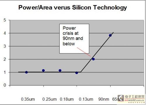
Prior to 0.13-micron technology, DSP designs were able to increase performance while reducing power, allowing more circuits to be packed into a single chip. This was achieved primarily by reducing size and lowering voltage. At 90-nanometer technology, all of this is no longer possible.
The problem now is trading performance for functionality, a situation that device manufacturers do not want to face: putting more circuits on a chip but reducing performance, or reducing the number of circuits but reducing functionality.
As the "power limit" situation continues, designers have been increasing power consumption to gain performance and functionality advantages. However, this brings a new risk: reaching the limit of heat dissipation. The resulting problems may already be present in the latest generation of general-purpose multi-core DSPs currently on the market.
Zero-sum game: static energy efficiency
Because performance is the primary goal for infrastructure, access, and EDGE applications, designers are generally not concerned with zero standby power. As a result, general-purpose silicon processes are often used to optimize performance, rather than selecting low-leakage silicon. Selecting low-leakage silicon reduces standby power, but also reduces speed and performance.
This requires selective use of transistors.
In battery-powered equipment, high voltage threshold (HVT) may be optimal; however, in infrastructure applications, standard voltage threshold (SVT) technology is preferred.
For example, if a design uses HVT logic and the supply voltage is 1.2V, it will generate 20mW of leakage power continuously. If it operates at maximum capacity, it will consume 1W of dynamic power.
The same design using SVT logic achieves nearly identical performance at a 1.0V supply voltage, generating four times more leakage power (100mW), but dissipating only 694mW of dynamic power (1.02 /1.22 = 0.694).
Therefore, the higher leakage SVT design consumes only 790 mW of total power, compared to 1.02 W for the HVT design, a 23% power saving.
Power consumption comparison between HVT design and SVT design
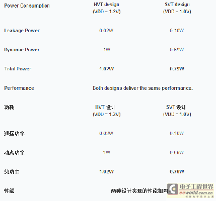
Although contrary to expectation, this example shows that using higher leakage SVT logic can save overall power compared to using lower leakage HVT logic due to the high switching activity in the latter circuit. This design is particularly useful for multiply and accumulate (MAC) circuits, but the opposite is true for circuits with low activity factors, such as RAM circuits or test circuits. Therefore, SVT logic is suitable for "always on" devices in the infrastructure.
Dynamic: Energy Efficiency Optimization
Clock trees and logic switching both contribute to dynamic energy consumption that must be handled in new generation multi-core DSPs. By continuously optimizing the design of these two energy consuming factors, energy efficiency can be greatly improved.
Clock trees (nets and buffers used to implement synchronous clocks to trigger the design) absorb some energy from the chip during their own triggering operations. Energy is also consumed in the process of charging and discharging the clock trees (which are usually large) that are spread throughout the latest high-speed chips. In addition, some new generation DSPs use faster clocks (1GHz or more), which requires larger actuators that consume more energy. If the clock propagation delay through the chip and the associated skew is to be minimized, larger actuators are required. This in turn consumes more energy.
Clock tree gating for reduced energy consumption
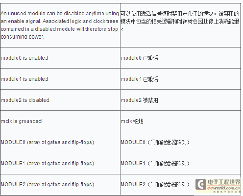
An unused module can be disabled anytime using an enable signal. Associated logic and clock trees contained in a disabled module will therefore stop consuming power.
Unused blocks can be disabled at any time using an activation signal. The associated logic and clock tree contained in the disabled block will therefore stop consuming energy.
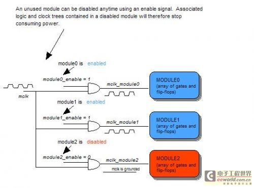
Equipment designers can reduce energy consumption in clock trees by combining the following proven techniques:
Individually enable clock triggers to limit the number of times an operation is triggered when timing is required.
Gated clock trees, which can dynamically block clocking of entire circuit segments when not in use.
Multi-loop path design can reduce the number of triggers and the frequency of triggers in the circuit.
Combine computational circuits where architecturally feasible, so that a series of MAC operations can be implemented in cascaded combinational circuits rather than synchronous feedback circuits. Borrowing multi-cycle path technology; this approach can greatly reduce the number of triggers used and reduce the trigger frequency.
Minimize the scope of flip-flops and circuits used, use physically smaller clock trees, and thus reduce the required stimulus buffers.
Finally, eliminating clock trees entirely can significantly reduce power consumption while increasing performance. Clockless design techniques can be applied to the logic circuits that consume the most power. Forward-thinking designers will actively pursue the above solutions. Clockless design is the most efficient and cost-effective way to resolve the ever-present conflict between performance and power.
Logic switching optimization
Logic switching plays a significant role in energy consumption because the overall energy consumption occurs during the charge and discharge process of the logic switching state transition. A combination of the following proven techniques can be used to minimize the energy consumption in logic switching.
Optimizing physical gates: This technique can achieve the greatest gains in energy efficiency metrics, especially for smaller chip size technologies. Although the principle is very simple, it is difficult to implement this technique using current layout tools and methods; because these tools and methods were originally developed to speed up product launches and sacrifice performance to increase the level and complexity of the design.
Eventually physical gates were invented, and some abstract language, such as VHDL, could be used to create chips based on the functional goals of the designer. This technology has both advantages and disadvantages. The current standard approach is to allow designers to avoid the details of the physical implementation, thereby speeding up the introduction of products.
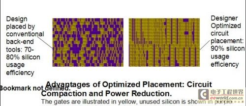
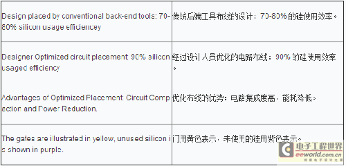
The downside of this technique is that designers of complex chips have no control over their designs, including the length of the wires, which can greatly increase the total capacitance of the circuit. Designers are still better than design tools at figuring out the best wire and circuit designs. Human judgment still has an advantage if mature techniques are used and the design details are deeply understood. Designers can also immediately see situations where subtle changes to the integrated circuit can reduce the length of the interconnect wires exponentially. In fact, documented information shows that human-intervened physical gate techniques can reduce the average length of circuit wires by up to half (compared to the same design implemented in the traditional best automatic back-end tools). Moreover, the circuit integration achieved by strategic routing can easily increase silicon utilization to more than 90%. This means that silicon utilization is improved by about 20% compared to the results using automatic back-end tools.
In addition, the gates that drive these very short lines are typically smaller and consume less power than an automatically wired and routed design. As a result, the entire circuit is smaller, faster, and consumes significantly less power than an automatically wired equivalent. When using only low-HVT logic elements in 90nm technology, this circuit integration technique allows the entire datapath engine to run at 1.5-2GHz while consuming up to 4x less power than a conventionally designed equivalent.
Optimizing long signal routing: Long signal routing can significantly improve performance when combined with other high-power, high-speed circuit elements. For example, a data bus may use long routes and change states frequently. Reducing the overall capacitance of such a line can greatly reduce power consumption, increase speed, and reduce buffering requirements. However, designers face the challenge of reducing capacitance by routing long signals with greater spacing while still allowing routing to close very dense portions of the design. Some of these tools and techniques include:
Eliminate circuits that make useless changes to state: Disable any circuit whose output will not be used after it is changed. This can be accomplished by using clock gating.
Reducing the number of high-frequency gates: PC processor chips (such as Pentium™ and other processors) have demonstrated that increasing functionality comes at the expense of increasing power consumption. The exponential increase in power consumption comes from increasing circuit performance using one or more of the following techniques:
Using a more complex circuit (i.e., using a look-ahead adder instead of a parallel adder) would take up more area and consume more energy;
Using larger gates, buffers, and actuators to speed up switching results in diminishing returns.
Often, equivalent performance can be achieved by using simpler, slower circuits that operate in parallel or take slow, multi-cycle paths, which can greatly reduce power consumption. However, contrary to what one might expect, such circuits often take up less overall area. In fact, even when used in parallel, they often have less total wiring. This is because, individually, they require fewer and smaller gates per instance than larger, faster, more power-hungry circuits.
• Reduce the size of voltage switching swings: Energy consumption can be further reduced by reducing the voltage switching swings through long bus and clock lines. This involves using balanced transmission line technology with small voltage swings, such as those used in high-performance memory designs (such as differential amplifiers). Such transmission lines operate with small voltage switching, which can greatly reduce energy consumption. Although this technology usually requires the use of intermediate voltage rails/planes in the chip, these transmission lines can change state at speeds up to 10 times the speed of traditional CMOS rail-to-rail lines; while consuming the same amount of energy, energy efficiency can be greatly improved.
• Plan the voltage operating range: Designers should exercise restraint when specifying their systems. Not every element in the system needs to be high performance, especially those that are not part of the 10% of functions that are critical to the entire system. In fact, it is acceptable to run the other 90% of functions as lean as possible. Therefore, designers should treat different parts of the circuit differently with different voltage rails. For example, 10% of the chip's circuits can be supplied with 1.2V to run at 3GHz, another 40% can be supplied with 1.0V to run at 1GHz, and the remaining 50% can be supplied with 0.8V to run at 400MHz. In the aggregate, the best overall energy efficiency metric achievable for a particular application can be achieved.
Controlling energy efficiency issues
As applications become more diverse and tools become more complex, designers of telecom access and infrastructure equipment struggle with how to build high-performance products at the right price and with a reasonable lifespan. However, the increasing refinement and specialization of chip design methodologies has put these technologies out of reach for many products. This difficulty is particularly acute for chips designed by large teams of dedicated engineering designers using best-in-class back-end design tools. Fortunately, there are a variety of techniques to manage the energy efficiency metrics of chips, achieving up to 3:1 MIPS/power ratios. These techniques range from the very simple to the extremely complex, offering a wide range of improvement possibilities.
Surprisingly, the most efficient techniques, such as optimizing wiring and routing, can be relatively simple techniques based on the designer's best judgment and intelligence if purpose-built tools are used.
Surprisingly, the most effective techniques, such as optimizing place and route, are relatively simple when using tools designed for that specific purpose and based on the designer's best judgment and wisdom.
Previous article:DSP Hardware and Software Design in IEEE1394 Video Vision System
Next article:Design of Wideband Step Frequency Signal Source Based on FPGA
Recommended ReadingLatest update time:2024-11-16 14:27


- Popular Resources
- Popular amplifiers
- Huawei's Strategic Department Director Gai Gang: The cumulative installed base of open source Euler operating system exceeds 10 million sets
- Analysis of the application of several common contact parts in high-voltage connectors of new energy vehicles
- Wiring harness durability test and contact voltage drop test method
- Sn-doped CuO nanostructure-based ethanol gas sensor for real-time drunk driving detection in vehicles
- Design considerations for automotive battery wiring harness
- Do you know all the various motors commonly used in automotive electronics?
- What are the functions of the Internet of Vehicles? What are the uses and benefits of the Internet of Vehicles?
- Power Inverter - A critical safety system for electric vehicles
- Analysis of the information security mechanism of AUTOSAR, the automotive embedded software framework
 Professor at Beihang University, dedicated to promoting microcontrollers and embedded systems for over 20 years.
- Innolux's intelligent steer-by-wire solution makes cars smarter and safer
- 8051 MCU - Parity Check
- How to efficiently balance the sensitivity of tactile sensing interfaces
- What should I do if the servo motor shakes? What causes the servo motor to shake quickly?
- 【Brushless Motor】Analysis of three-phase BLDC motor and sharing of two popular development boards
- Midea Industrial Technology's subsidiaries Clou Electronics and Hekang New Energy jointly appeared at the Munich Battery Energy Storage Exhibition and Solar Energy Exhibition
- Guoxin Sichen | Application of ferroelectric memory PB85RS2MC in power battery management, with a capacity of 2M
- Analysis of common faults of frequency converter
- In a head-on competition with Qualcomm, what kind of cockpit products has Intel come up with?
- Dalian Rongke's all-vanadium liquid flow battery energy storage equipment industrialization project has entered the sprint stage before production
- Allegro MicroSystems Introduces Advanced Magnetic and Inductive Position Sensing Solutions at Electronica 2024
- Car key in the left hand, liveness detection radar in the right hand, UWB is imperative for cars!
- After a decade of rapid development, domestic CIS has entered the market
- Aegis Dagger Battery + Thor EM-i Super Hybrid, Geely New Energy has thrown out two "king bombs"
- A brief discussion on functional safety - fault, error, and failure
- In the smart car 2.0 cycle, these core industry chains are facing major opportunities!
- The United States and Japan are developing new batteries. CATL faces challenges? How should China's new energy battery industry respond?
- Murata launches high-precision 6-axis inertial sensor for automobiles
- Ford patents pre-charge alarm to help save costs and respond to emergencies
- New real-time microcontroller system from Texas Instruments enables smarter processing in automotive and industrial applications
- The problem of interference between ADC channels of STM32
- Where does the chip's power come from?
- EEWORLD University Hall ---- Zhou Gong Series Lectures —— CAXA Electronic Chart Example
- 8266 WiFi module obtains time and weather information through the network
- Performance Differences Between DC-DC Switching Power Supplies and DC-DC Integrated Modules
- Power Issues
- BlueNRG2 sends 247 bytes at a time
- AUTOSAR’s popularity in automotive electronics software development
- Understand the perfect combination of RPA and AI in one article
- X-nucleo-iks01A3 application--using Lis2DW12 accelerometer to calculate angle

 MATLAB and FPGA implementation of wireless communication


 京公网安备 11010802033920号