Taiwan's Industrial Technology Research Institute (ITRI) has proposed an innovative method that can significantly improve the efficiency of customized FPGA prototype verification, automate existing in-circuit emulation debugging functions, and provide higher FPGA visibility. This FPGA-based SoC verification platform is a promising new field for ITRI.
Case Study: High-Performance Multimedia SoC Platform
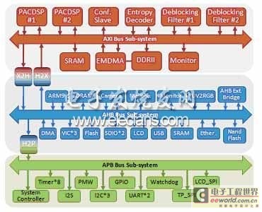
This SoC design is a high-performance Android-compatible multimedia SoC platform. It is equipped with AXI, AHB and APB buses for communication; high-performance customized IP components designed by ITRI (PACDSPs, EMDMA and DDR2 controllers) are connected to the AXI bus to accelerate the execution of multimedia application software such as H.264 video codec. Standard IP components including ARM, SDRAM, DMA, SRAM, Ethernet and LCD are connected to the AHB bus for general applications. Finally, low-frequency IP blocks such as UART, Timer, I2S, I2C and Watchdog are connected to the APB bus.

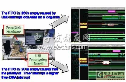
The following case study illustrates how ITRI and Siyuan Technology engineers collaborated to overcome verification challenges in ITRI’s SoC designs using Siyuan Technology’s ProtoLink Probe Visualizer. The problem was related to the sound function: the function worked properly (recording and playback) without an OS activated on the FPGA prototype board, but did not work properly when Linux was enabled on the prototype board. Using traditional debugging methods to troubleshoot this type of problem in an FPGA prototype environment is difficult. The FPGA’s visibility is limited to a few signals and clock cycles, which does not provide enough information to find the error. And because it takes a long time to activate an OS (such as Linux), trying to solve the problem through register translation level (RTL) simulation is not feasible. Because the cause of the problem may be in the software, hardware, or driver, it is a challenge to determine the root cause of the problem.
A different approach
To simplify debugging, a more efficient verification method is needed. ProtoLink Probe Visualizer is a new prototype verification environment that uses a software-based approach to provide a high level of design visibility from the RTL design stage to the final design implementation stage, which can fully accelerate the debugging process.
ITRI was initially concerned that its custom prototype board might not meet the interface requirements of Siyuan Technology's ProtoLink Probe Visualizer. After a few quick tests, Siyuan Technology engineers proved that the standard J connector on ITRI's custom prototype board could be successfully connected to the workstation running the Probe Visualizer software. Simply add a phase-locked loop (PLL) to the prototype board to provide the required sampling clock. The FPGA setup process is very simple and can be easily integrated into existing programs (scripts). Automatically select about 100 probed signals, which is 6 times the visibility of previous methods. In addition, all probe data can be stored in the external 2GB probe signal memory without occupying FPGA resources. The actual additional probe logic only occupies 2% of the FPGA, which is quite small. The data capacity of the external memory can store sufficient length of clock cycles, allowing engineers to truly understand the relationship between software, hardware and drivers.
The ITRI team used the stored probe data to perform debugging operations through the advanced observation, tracking and analysis functions of the Verdi automatic debugging system of Siyuan Technology. After repeated debugging, two problems were found: 1) The USB interrupt locked the ARM for a long time, so the FIFO in I2S was empty, which caused the problem; 2) The timer interrupt had a higher priority than the DMA interrupt, which once again caused the FIFO in I2S to be empty. ITRI engineers used the debugging function of Siyuan Technology's software to further analyze the design behavior. Although it showed common error symptoms, the engineers were able to quickly discover that the root cause of these errors originated from two different situations.

In addition, observing additional key signals is necessary for debugging, but most of these signals are not in the original probe list. ITRI engineers can quickly probe the ECO process through Probe Visualizer, adding 10 new signals in 10 minutes without recompiling the entire design. Compared with traditional debugging methods that require dragging new signals in RTL and re-performing synthesis and placement and routing operations for this specific design, which takes about 2 to 3 hours, this innovation saves a lot of time.
Engineers can easily drag the required additional RTL probe signals from the Verdi debugging environment to ProbeVisualizer. This system automatically establishes the signal correspondence from RTL to the logic gate layer (RTL-to-gate level), so you can quickly perform some routing operations directly on the FPGA layout and routing files to see the newly added probe signals, greatly shortening the debugging operation time, so you can handle multiple debugging work stages (debug session) in a short time. For the "black box" IP blocks used in the design, you only need the EDIF name to perform the detection ECO process.
Evaluation results
After correcting the issues and successfully trial-producing the design, ITRI engineers reviewed the actual time spent on the project and evaluated the results of this new FPGA SoC prototyping method.
The time for RTL design, simulation, communication protocol verification and FPGA design implementation was about 2 months. The time spent on driver porting was much shorter, only about 2 weeks. The engineers then spent another 2 months on verification, trying to solve the sound problem by checking the internal signals of the FPGA through a hardware logic analyzer, and also adding observation points in the sound driver to connect and try to find the problem. This traditional FPGA debugging method takes as long as the design and development time, but for the ITRI team, it is quite frustrating that the results are still nothing. However, after the application software education training/support courses provided by Siyuan Technology and a week of hands-on experience, ITRI engineers used ProtoLink Probe Visualizer to clarify the two major problems in just one week!
For ITRI, ProtoLink Probe Visualizer is a very effective method for debugging FPGA prototype boards. Engineers are no longer limited to traditional debugging methods, and adding observation points in real-time application software may also cause other problems. By maintaining the original software and monitoring the real-time RTL behavior of more FPGA signals in millions of clock cycles, users can get the visibility they need to better understand and debug design problems more easily.

In summary, Sieyuan Technology's Probe Visualizer has changed the way prototype boards are verified through an innovative software-based approach, achieving rich, real-time design visibility and enabling prototype boards to use the debugging power of Verdi, significantly reducing the prototype board debugging time by half compared to traditional methods.
Previous article:Research on Turbo Decoding and Its DSP Implementation
Next article:Design of TV aiming and viewing system based on DSP and FPGA
- Popular Resources
- Popular amplifiers
- Huawei's Strategic Department Director Gai Gang: The cumulative installed base of open source Euler operating system exceeds 10 million sets
- Analysis of the application of several common contact parts in high-voltage connectors of new energy vehicles
- Wiring harness durability test and contact voltage drop test method
- Sn-doped CuO nanostructure-based ethanol gas sensor for real-time drunk driving detection in vehicles
- Design considerations for automotive battery wiring harness
- Do you know all the various motors commonly used in automotive electronics?
- What are the functions of the Internet of Vehicles? What are the uses and benefits of the Internet of Vehicles?
- Power Inverter - A critical safety system for electric vehicles
- Analysis of the information security mechanism of AUTOSAR, the automotive embedded software framework
 Professor at Beihang University, dedicated to promoting microcontrollers and embedded systems for over 20 years.
- Innolux's intelligent steer-by-wire solution makes cars smarter and safer
- 8051 MCU - Parity Check
- How to efficiently balance the sensitivity of tactile sensing interfaces
- What should I do if the servo motor shakes? What causes the servo motor to shake quickly?
- 【Brushless Motor】Analysis of three-phase BLDC motor and sharing of two popular development boards
- Midea Industrial Technology's subsidiaries Clou Electronics and Hekang New Energy jointly appeared at the Munich Battery Energy Storage Exhibition and Solar Energy Exhibition
- Guoxin Sichen | Application of ferroelectric memory PB85RS2MC in power battery management, with a capacity of 2M
- Analysis of common faults of frequency converter
- In a head-on competition with Qualcomm, what kind of cockpit products has Intel come up with?
- Dalian Rongke's all-vanadium liquid flow battery energy storage equipment industrialization project has entered the sprint stage before production
- Allegro MicroSystems Introduces Advanced Magnetic and Inductive Position Sensing Solutions at Electronica 2024
- Car key in the left hand, liveness detection radar in the right hand, UWB is imperative for cars!
- After a decade of rapid development, domestic CIS has entered the market
- Aegis Dagger Battery + Thor EM-i Super Hybrid, Geely New Energy has thrown out two "king bombs"
- A brief discussion on functional safety - fault, error, and failure
- In the smart car 2.0 cycle, these core industry chains are facing major opportunities!
- The United States and Japan are developing new batteries. CATL faces challenges? How should China's new energy battery industry respond?
- Murata launches high-precision 6-axis inertial sensor for automobiles
- Ford patents pre-charge alarm to help save costs and respond to emergencies
- New real-time microcontroller system from Texas Instruments enables smarter processing in automotive and industrial applications
- Please ask senior programmers to help look at this problem
- How to use MSP430 to implement PWM signal
- Internal circuits of CH551, CH552, CH554, CH559
- [Zero-knowledge ESP8266 tutorial] Quick start 29 How to use the nine-axis sensor module
- Application issues of optocouplers in switch acquisition
- Noise Countermeasure Solution for Quick Charging Circuit
- MicroPython adds self-power and power consumption parameters to USB
- Are you tossing and turning over the issue of isolated transceivers? We will tell you everything we know!
- (1) Unpacking and setting up the IAR environment
- When do you use the RF interface? When do you use the Bluetooth interface?

 Electronic system level platform design
 Multiprocessor+Systems-on-Chips


 京公网安备 11010802033920号