1 Introduction
Saturable inductor is an inductor with high hysteresis loop squareness ratio, high initial permeability, small coercive force and obvious magnetic saturation point. It is often used as a controllable delay switch element in electronic circuits. Due to its unique physical properties, saturable inductor has also been increasingly widely used in high-frequency switching power supply switching noise suppression technology and large current output auxiliary circuit voltage stabilization technology.
2 Basic physical characteristics of saturable inductors
Figure 1(a) and Figure 1(b) are the hysteresis loops of ordinary ferrite inductors and saturable inductors, respectively. From the comparison between the two, it can be clearly seen that the saturable inductor has the characteristics of high hysteresis loop rectangular ratio (Br/Bs), high initial magnetic permeability mi, low coercive force Hc, obvious magnetic saturation point (A, B), etc. In addition, it can be seen from Figure 1(b) that the area surrounded by the hysteresis loop of the saturable inductor is small, so the high-frequency hysteresis loss of the saturable inductor is correspondingly small. Since saturable inductors are usually made of ferromagnetic materials such as microcrystalline, amorphous, and Permalloy, saturable inductors generally have very high initial magnetic permeability mi and very high saturation magnetic induction.
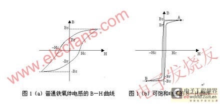
Strength Bs. Due to the difference in physical properties, saturable inductors have two significant differences from ordinary ferrite inductors in terms of application:
(1) Since the saturation magnetic field strength is very small, the energy storage capacity of the saturable inductor is very weak and cannot be used as an energy storage inductor. The theoretical value of the maximum energy storage Em of the saturable inductor can be expressed by the following formula:
Em=m·H2·V/2 (1)
Where: m: critical saturation point magnetic permeability; H: critical saturation point magnetic field intensity; V: effective volume of magnetic material.
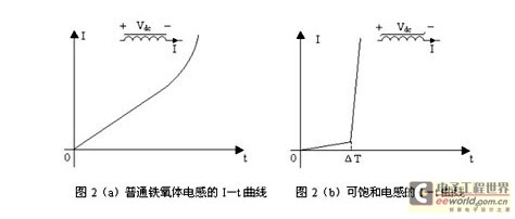
(2) Since the initial magnetic permeability of the saturable inductor is high and the magnetic resistance is small, the inductance coefficient and inductance are both large. When the external voltage is applied, the initial current inside the inductor increases slowly. Only after the delay time DT, when the current in the inductor coil reaches a certain value, the saturable inductor will immediately saturate. It has a very obvious switching characteristic, so it is often used as a controllable delay switching element in the circuit. This switching characteristic of the saturable inductor is not possessed by ordinary ferrite inductors.
The curves of the current intensity I of the common ferrite inductor and the saturable inductor changing with time t under the action of the DC voltage Vdc are shown in FIG2(a) and FIG2(b).
3 Switching noise suppression effect of saturable inductors
Switching power supplies usually operate in the frequency range of tens of kilohertz to hundreds of kilohertz. The rectifier diodes on the secondary side of the power supply will flow through a large reverse recovery current during the high-frequency shutdown process. Therefore, the power supply conduction spike noise formed is an important part of the switching power supply noise. Trying to reduce the reverse recovery current of the rectifier diodes, thereby reducing the conduction and radiation noise of the switching power supply is an important aspect of switching power supply design.
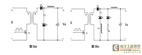
In the forward power supply circuit shown in Figure 3(a), when the primary power tube V1 starts to conduct, the secondary rectifier diode D1 starts to conduct, and D2 starts to cut off, due to the charge storage effect of the diode PN junction, a reverse recovery spike current i with a large current change rate di/dt flows through D2, causing corresponding spike currents to flow through V1 and D1. Under the combined effect of leakage inductance, line inductance and other factors, high-frequency conduction noise will be generated at the power supply output. The greater the reverse voltage applied to D2, the longer the reverse recovery time of D2, the greater the reverse recovery current change rate di/dt, and the greater the power supply output noise. A large reverse recovery spike current will not only generate power supply noise, but also easily damage the rectifier device.
When the primary power tube V1 starts to cut off, the secondary rectifier diode D1 starts to cut off, and D2 starts to conduct and continue current, due to the same reason, high-frequency shutdown noise will also be generated at the output end of the power supply. The shutdown noise is usually much smaller than the conduction noise and is generally not considered as a key point in power supply design.
In order to effectively reduce the reverse recovery current of the rectifier diode and suppress the reverse recovery current change rate, the measures usually taken in power supply design are: select Schottky diodes with no PN junction charge storage effect and very short reverse recovery time, or select rectifier diodes with small reverse recovery current change rate and soft recovery characteristics as secondary rectifier devices; add RC buffer circuits at both ends of the rectifier diode, or connect a small inductor in series with the rectifier diode to soften the change rate of the switching voltage or reverse recovery current. Since the saturable inductor has the characteristics of large inductance, easy saturation, and weak energy storage, it is very suitable to be connected in series with the rectifier diode as a current limiting inductor, so that the amplitude and change rate of the reverse recovery current of the rectifier diode are limited to a reasonable range.
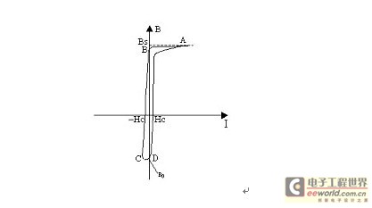
In the circuit shown in Figure 3(b), when V1 starts to conduct, D1 starts to conduct, and D2 starts to cut off, due to the current limiting effect of the saturable inductor Ls, the amplitude and rate of change of the reverse recovery current flowing through D2 will be significantly reduced, thereby effectively suppressing the generation of high-frequency conduction noise. In the process of diode D2 being turned on, off, and on, the change of magnetic induction intensity in Ls is shown in Figure 4. In the reverse recovery process of the current in D2 from forward current, zero current, maximum reverse current to zero current, the corresponding magnetic induction intensity in Ls is located at points A, B, C, and D in Figure 4. After the diode D2 is turned on, the corresponding magnetic induction intensity will transition from point D to point A again. When D2 changes from cutoff to on and on, due to the turn-on delay time DT of Ls, this will affect the freewheeling effect of D2 and generate a negative peak voltage at the negative pole of D2. Adding auxiliary diode D3 and resistor R1 to the circuit can better solve this problem.
4 Application of saturable inductor in magnetic amplifier voltage regulation technology
Magnetic amplifier voltage regulation is a method of controlling the duty cycle and output power of a switching power supply and stabilizing the output voltage of the power supply by using the physical characteristics of the conduction delay of a saturable inductor. By adding appropriate sampling and control elements to the saturable inductor and adjusting its conduction delay time, the most common magnetic amplifier voltage regulation circuit can be formed. Figure 5 is a dual-tube forward switching voltage regulator with an input of 110Vac~220Vac/50HZ and an output of 5Vdc/20A and 12Vdc/10A, in which 5V is the main control circuit. The auxiliary 12V output current is relatively large, and there are high requirements for voltage regulation accuracy and load stability. The voltage regulation effect of ordinary methods is not very ideal. If the magnetic amplifier voltage regulation technology is used, this problem can be satisfactorily solved, making the structure of the voltage regulation circuit simple, the power dissipation small, and the voltage regulation accuracy of the millivolt level can be achieved.
After the 110Vac~220Vac/50HZ input is boosted by the active power factor correction circuit, the output DC voltage of 400Vdc is added to the primary of the power module. The secondary winding N1 outputs a square wave voltage with a peak value of 20V and a duty cycle of about 25%, and the output peak voltage of the secondary winding N2 is 50V. Before adding the magnetic amplifier voltage stabilization circuit (the dotted box in Figure 5), the output voltage V2»50V´0.25=12.5V at the auxiliary circuit 12V, when 5V is fully loaded and 12V is unloaded, the actual output voltage will be much higher because the auxiliary circuit has no dead load discharge circuit. After adding the magnetic amplifier voltage stabilization circuit, due to its regulation function, the auxiliary circuit can obtain an ideal 12V output voltage under any load condition. The working principle of the magnetic amplifier voltage stabilization circuit is analyzed below. The magnetic induction intensity change curve of the saturable inductor Ls during the voltage stabilization process can still be represented by Figure 4.
When the primary power tubes V1 and V2 are turned off, the secondary diode D1 is reversely turned off, the diode D2 is turned on for freewheeling, the energy storage inductor L1 releases energy, and the auxiliary circuit of the power supply is in the off state. At this time, a small current If of the milliampere level flows into the saturable inductor Ls through Q1 and D3, generating an additional magnetic induction intensity B0 in Ls, and B0 is located at point V of the hysteresis loop. After the power tubes V1 and V2 are turned on again, due to the current limiting effect of the inductor Ls, the current in D1 can only increase slowly, D2 still plays a role of freewheeling, and the auxiliary circuit of the power supply is still in the off state. Only after the delay time DT, when the current in D1 increases to a certain value and the magnetic induction intensity in Ls reaches the saturation magnetic induction intensity BS (point A), Ls will be saturated immediately, the current in D1 will increase rapidly, D2 will be turned off quickly, the energy storage inductor L1 will enter the energy storage stage, and the auxiliary circuit of the power supply will enter the on state.
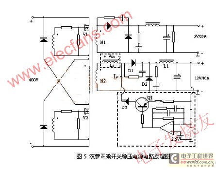
From the above analysis, we can see that due to the insertion of the saturable inductor Ls, the on-time T'ON and duty cycle a' of the auxiliary circuit are smaller than those of the main circuit. By adjusting the duty cycle a', the purpose of output voltage regulation of the auxiliary circuit is finally achieved. a' has a large adjustment range. When the auxiliary circuit is completely unloaded, a' can be adjusted to almost 0, so that the auxiliary circuit has a high load stability and voltage regulation accuracy. The duty cycle a' can be calculated according to the following formula:
a´= T´ON/T=(TON-DT)/T (2)
Where: TON: the on-time of the main circuit; T: the switching cycle of the power supply; DT: the on-delay time of Ls.
The conduction delay time DT of the saturable inductor is determined by the additional magnetic induction intensity B0, current If, etc. B0 and If are automatically adjusted by the sampling control circuit according to the output voltage. DT is given by the following formula:
DT=N´Ae´(BS-B0)/Vin (3)
Where: BS: saturation magnetic induction of saturable inductor; B0: between ±BS, determined by the operating current If;
Ae: cross-sectional area of saturable inductor; N: number of turns of saturable inductor coil;
Vin: The voltage applied across the saturable inductor.
When B0=-BS, DT has a maximum value DTmax=2N´Ae´BS/Vin; when B0=Br, DT has a minimum value DTmin= N´Ae´ (BS-Br)/Vin. If is generally designed to be tens of milliamperes, and the approximate value of If is given by the following formula:
If »(HC- B0/mi)´lm/N (4)
Where: HC: coercive force of saturable inductor; mi: initial magnetic permeability; lm: equivalent magnetic path length of saturable inductor.
Based on the same principle as the auxiliary output voltage regulation of the forward power supply, two sets of magnetic amplifier voltage regulation circuits can form the auxiliary output voltage regulation unit of the push-pull power supply and bridge power supply. In addition, the magnetic amplifier can also be conveniently used to form the auxiliary output voltage regulation unit of the forward and reverse mixed power supply, etc., which will not be described here one by one.
5 Conclusion
This article introduces the basic physical characteristics of saturable inductors and the switching noise suppression effect of saturable inductors, focuses on analyzing the working principle of magnetic amplifier voltage regulator circuits, and proposes several theoretical calculation formulas. In the actual engineering design of power supplies, since suppliers usually provide empirical design formulas for saturable inductors and magnetic amplifiers, the actual design work is relatively simple and easy. The requirements for circuit parameters of the magnetic amplifier voltage regulator circuit are not very strict, and under normal circumstances, very good voltage regulation effects can be achieved.
Previous article:What is a film capacitor
Next article:CFL energy-saving lamps
- Popular Resources
- Popular amplifiers
- High signal-to-noise ratio MEMS microphone drives artificial intelligence interaction
- Advantages of using a differential-to-single-ended RF amplifier in a transmit signal chain design
- ON Semiconductor CEO Appears at Munich Electronica Show and Launches Treo Platform
- ON Semiconductor Launches Industry-Leading Analog and Mixed-Signal Platform
- Analog Devices ADAQ7767-1 μModule DAQ Solution for Rapid Development of Precision Data Acquisition Systems Now Available at Mouser
- Domestic high-precision, high-speed ADC chips are on the rise
- Microcontrollers that combine Hi-Fi, intelligence and USB multi-channel features – ushering in a new era of digital audio
- Using capacitive PGA, Naxin Micro launches high-precision multi-channel 24/16-bit Δ-Σ ADC
- Fully Differential Amplifier Provides High Voltage, Low Noise Signals for Precision Data Acquisition Signal Chain
- Innolux's intelligent steer-by-wire solution makes cars smarter and safer
- 8051 MCU - Parity Check
- How to efficiently balance the sensitivity of tactile sensing interfaces
- What should I do if the servo motor shakes? What causes the servo motor to shake quickly?
- 【Brushless Motor】Analysis of three-phase BLDC motor and sharing of two popular development boards
- Midea Industrial Technology's subsidiaries Clou Electronics and Hekang New Energy jointly appeared at the Munich Battery Energy Storage Exhibition and Solar Energy Exhibition
- Guoxin Sichen | Application of ferroelectric memory PB85RS2MC in power battery management, with a capacity of 2M
- Analysis of common faults of frequency converter
- In a head-on competition with Qualcomm, what kind of cockpit products has Intel come up with?
- Dalian Rongke's all-vanadium liquid flow battery energy storage equipment industrialization project has entered the sprint stage before production
- Allegro MicroSystems Introduces Advanced Magnetic and Inductive Position Sensing Solutions at Electronica 2024
- Car key in the left hand, liveness detection radar in the right hand, UWB is imperative for cars!
- After a decade of rapid development, domestic CIS has entered the market
- Aegis Dagger Battery + Thor EM-i Super Hybrid, Geely New Energy has thrown out two "king bombs"
- A brief discussion on functional safety - fault, error, and failure
- In the smart car 2.0 cycle, these core industry chains are facing major opportunities!
- The United States and Japan are developing new batteries. CATL faces challenges? How should China's new energy battery industry respond?
- Murata launches high-precision 6-axis inertial sensor for automobiles
- Ford patents pre-charge alarm to help save costs and respond to emergencies
- New real-time microcontroller system from Texas Instruments enables smarter processing in automotive and industrial applications
- Share an open source software download URL
- "Practice Together in 2021" + Looking Forward
- Senior foreigner explains the misunderstandings of high-speed PCB design and testing (video-Chinese)
- After zigbee sends data to nb-iot, nb-iot sends data to the cloud, but the data displayed on the cloud is completely wrong. How to solve it?
- Notice: The new markdown editor is now online!!
- Design of password lock using AT89S52 single chip microcomputer
- [Review of Arteli Development Board AT32F421] + Have a good understanding of the power supply voltage
- 【Development and application based on NUCLEO-F746ZG motor】4. Share information
- encryption
- Motor control basics - timer basics and PWM output principles

 NJM4559E-(TE1)


 京公网安备 11010802033920号