introduction
Although the 5-channel circuit introduced in this article uses only one MAX5927A 4-channel hot-swap controller, it can implement the hot-swap function of 3 positive power supplies and 2 negative power supplies. The circuit in Figure 1 meets the following load power supply and power-up sequencing requirements:- Ch1 = +3.3V at 2A (circuit powers down at ≥ 3A)
- Ch2 = +5V at 1.6A (circuit powers down at ≥ 2.4A)
- Ch3 = +12V at 2A (circuit de-energizes at ≥ 3A)
- At 150mA, Ch4 = -12V (no circuit power-off action)
- At 50mA, Ch5 = -5V (no circuit power-off action)
- The startup sequence is: Channel 2 (+5V) and Channel 3 (+12V) turn on immediately when the active-low CARD_PRESENT goes low. STAT2 and STAT3 go high 10.8ms after the active-low CARD_PRESENT goes low.
- Channel 1 (+3.3V) turns on with a delay of 11.8ms relative to Channel 2 and Channel 3. STAT1 goes high 10.8ms after Channel 1 turns on.
- Channel 4 (-12V) and Channel 5 (-5V) are turned on with a delay of 27.8ms relative to Channel 2 and Channel 3. STAT4 goes high 10.8ms after Channel 4 and Channel 5 are turned on.
- Latched fault management. If an error occurs on any of Channel 1 to Channel 3, all channels are shut down until the next active-low CARD_PRESENT off and on cycle.

Figure 1. 5-channel hot-swap circuit controls 3 positive and 2 negative supplies
Although the delay requirements and fault management are specific to this design, the delay can be changed to meet other timing requirements. If desired, the fault management can be changed to an automatic retry mode.
Hot Swap Controller Selection
The MAX5927A was chosen because of its exceptional +15V absolute maximum input voltage, compared to the 14V for the MAX5927. This voltage advantage is important if the 12V supply circuit uses a mirror-circuit inductor that could cause supply voltage ringing and overshoot if the circuit breaker opens during an overload.Turn-on timing
Resistor R36 (at IC pin 10) sets the on-time for each channel to 10.8ms ±2.8ms. During this time, the MAX5927A's internal slow comparator is disabled, allowing the load capacitor to charge to twice the preset current trigger value for each channel, Channel 1 through Channel 3, to meet the requirement. During this time, the circuit breaker does not need to be tripped, and the load capacitor can easily charge to its final value. Adjusting R36 between 4kΩ and 500kΩ allows the startup delay to be set to any value between 400µs (minimum) and 50ms (maximum). At the end of this startup time, the STAT output transitions from FALSE to TRUE. The STAT output is positive, but can be set to negative by grounding POL (pin 29).Channel 1 turns on with a delay of 11.8ms relative to Channel 2 and Channel 3 by the (R29 + R30) - C16 time constant; C16 can be increased to increase the delay. STAT1 goes high 10.8ms after Channel 1 begins turning on.
Channel 4 and Channel 5 are turned on 28ms later than Channel 2 and Channel 3 by the (R29 + R31) - C17 time constant; C17 can be increased to increase the delay, or R31 can be decreased to decrease the delay. STAT4 goes high 10.8ms after Channel 4 and Channel 5 begin to turn on.
MODE is set (Pin 28 is turned on) to configure the MAX5927A for power-up sequencing mode.
Output voltage slew rate
The output voltage slew rate for all channels is set to approximately 1V/ms, independent of the load capacitor (C11 to C15) values. The gate capacitor values of C6 to C10 can be modified to change the slew rate. The slew rate is calculated as ΔV/Δt = IGATE/CGATE. This equation is not very accurate because the FET gate capacitance is not included in the calculation. The gate charging current for GATE1, GATE2, and GATE3 is approximately 100µA. The gate charging current for Q4 and Q5 is 30µA to 50µA due to the currents of R10 and R11. The load capacitor charging current can be calculated as ICHARGE = CLOAD × ΔV/Δt. It is given by IGATE/CGATE = ICHARGE/CLOAD. Capacitors C8 to C10 enable the outputs of Channels 1 to 3 to swing approximately 1V/ms. Without load, C13 to C15 charge at approximately 0.5A until the full output is reached. Without C8 to C10, the output charges the load capacitor with a current twice the current trigger value calculated above. Capacitors C6 and C7 are 10nF, which makes the swing of Channel 4 and Channel 5 approximately 1V/ms.Circuit breaker threshold
The slow comparator threshold of 21mV to 27.5mV and R7 = R9 = 8.3mΩ set the current limit for Channel 1 (+3.3V) and Channel 3 (+12V). The default value multiplied by 1.13 and R33 = R35 = 1.15kΩ gives a final value of approximately 3.1A to 3.8A. The slow comparator threshold of 21mV to 27.5mV and R8 = 10mΩ sets the current limit for Channel 2 (+5V). The default value multiplied by 1.15 and R34 = 1.18kΩ gives a final value of approximately 2.415A to 3.625A. Other current limit values are set by adjusting the sense resistors R7 to R9 and the ISET resistors R33 to R35. The default multipliers can be determined from the curves provided in the data sheet. The current limit circuit breaker does not provide protection for low current Channel 4 (-12V) and Channel 5 (-5V).Internal pullups pull LATCH high, configuring the MAX5927A for latched fault management. If a fault occurs on any of Channels 1 to 3, all channels are shut down until the next shut-down and turn-on cycle is initiated by an active-low CARD_PRESENT.
Negative voltage channel 4 and channel 5
The MAX5927A is designed to control positive-voltage circuits. However, negative-voltage channels Q4 and Q5 can be driven with approximately 4.2V gates from the MAX5927A’s GATE4 output , which is modified by transistors Q5 and Q6 and resistors R4–R7.The gate-charging current output of GATE4 is 60µA to 100µA, but is split to 30µA to 50µA in the symmetrical circuits R4–Q7 and R5-Q6. The voltage at GATE4 can be 5.3V above VIN4 (3.3V), or ≤+8.6V when on, and close to 0V when off. When on, VQ6(BASE) = VQ7(BASE) = 3.3V, and VQ6(EMITTER) = VQ7(EMITTER) ≈ 3.9V, and when off, it is 0V. The equal voltage drops across R4 and R5 allow Q6 and Q7 to share the current equally. Equal currents in R6 and R7 produce equal gate drives on Q4 and Q5. In the off state, the gate drive is 0 V when GATE4 = 0 V. The turn-off speed of Q4 and Q5 depends on the gate discharge current flowing through R6 to R7.
FET Selection
All channels, except the +12V channel, use n-channel MOSFET pass transistors in SOT23 packages; each FET schematic lists the maximum RDS(ON) at VGS = 4.5V and TJ = +25°C. A MOSFET with VGS(max) = 20V (Si9410) is used for the +12V channel.Summarize
The circuit meets all the load and power-sequencing design requirements—handling three positive and two negative voltage channels with proper sequential turn-on timing, overcurrent trip points greater than the required minimum, and an output slew rate of approximately 1V/ms—which is what the design requires.+3.3V delay for +5V and +12V channels = 11.8ms (see Figure 2)
-5V delay for +3.3V channel = 16.2ms (see Figure 3)
-5V load turn-off time = 1ms (see Figures 4 and 5)
-12V load turn-off time = 4ns (see Figures 6 and 7)
-12V output voltage slew rate ≈ 1V/ms (see Figure 8)
-12V load capacitor charging current ≈ 80mA (see Figure 9)
-5V output voltage slew rate ≈ 1V/ms (see Figure 10)
-5V load capacitor charging current ≈ 55mA (see Figure 11)
+3.3V output voltage slew rate ≈ 1V/ms (see Figure 12)
+3.3V load capacitor charging current ≈ 400mA (see Figure 12)
3A load +3.3V turned on without tripping circuit breaker (see Figure 13)
+3.3V circuit breaker turns off at 3.22A (see Figure 14)
+5V load capacitor charging current ≈ 500mA (see Figure 15)
+5V output voltage slew rate ≈ 1V/ms (see Figure 15) +
5V turns on at 2.4A load and does not trip the circuit breaker (see Figure 16)
+5V circuit breaker turns off at 2.87A (see Figure 17)
+12V load capacitor charging current ≈ 500mA (see Figure 18)
+12V turns on at 3A load and does not trip the circuit breaker (see Figure 19)
+12V circuit breaker turns off at 3.1A (see Figure 20)
+5V activates short circuit at ≈ 4A (see Figure 21)
+12V activates short circuit at ≈ 5.7A (see Figure 22)
Test Results
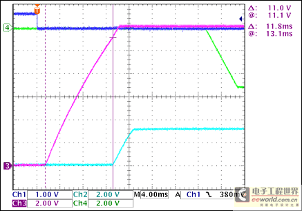
Figure 2. +12V to +3.3V Turn-On Delay, No LoadCh1
= Q8BASE(CARD_PRESENT), Ch2 = +3.3VOUT, Ch3 = +12VOUT, Ch4 = -5VOUTNote
: There is a 11.8ms delay between +12VOUT and +3.3VOUT.

Figure 3. +3.3V to -5V Turn-On Delay, No LoadCh1
= Q8BASE, Ch2 = +3.3VOUT, Ch3 = +12VOUT, Ch4 = -5VOUTNote
: There is a 16.2ms delay between +3.3VOUT and -5VOUT.

Figure 4. -5V Gate Turns Off Relative to +3.3VGATE, No LoadCh1
= Q8BASE, Ch2 = +3.3VGATE, Ch3 = +5VGATE, Ch4 = -5VGATENote
: The -5V gate turns off slowly; the FET turns off when 1 < VGATE < 3V (2.5V, typical). Thus, the -5V gate turns off completely 1.5ms to 4ms after the positive voltage channel turns off.
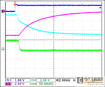
Figure 5. -5V Load Turns Off, 50mA LoadCh1
= Q8BASE, Ch2 = -5VGATE, Ch3 = -5VOUT, Ch4 = IIN(-5V)
Note: Although VOUT(-5V) does not reach 0V due to the discharge of the output capacitor, -5V falls to zero within 1ms.

Figure 6. -12V Gate Turn-Off, No LoadCh1
= Q8BASE, Ch2 = +3.3VGATE, Ch3 = +12VGATE, Ch4 = -12VGATENote
: The -12V gate turns off slowly; the FET turns off when 1 < VGATE < 3V (2.5V, typical). Thus, the -12V gate turns off completely 1ms to 4ms after the positive voltage channel turns off.
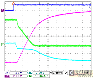
Figure 7. -12V Load Turn-Off, 150mA LoadCh1
= Q8BASE, Ch2 = -12VGATE, Ch3 = -12VOUT, Ch4 = IIN(-12V)
Note: Although VOUT(-12V) does not reach 0V due to the discharge of the output capacitors, the -12V input drops to zero within 4ms.

Figure 8. -12V Turn-On Waveforms
Ch1 = Q8BASE, Ch2 = -12VGATE, Ch3 = -12VOUT, Ch4 = IIN(-12V)
Note: Turn-On Sequence, 80Ω Resistive Load = 150mA
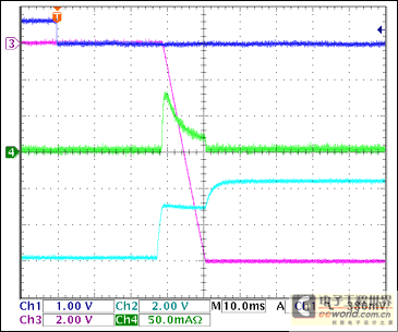
Figure 9. -12V Turn-On Waveforms, No Load
Ch1 = Q8BASE, Ch2 = -12VGATE, Ch3 = -12VOUT, Ch4 = IIN(-12V)
Note: IIN(PK) = 80mA, charging the output capacitors
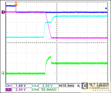
Figure 10. -5V Turn-On Waveforms, 100Ω Resistive Load = 50mA
Ch1 = Q8BASE, Ch2 = -5VGATE, Ch3 = -5VOUT, Ch4 = IIN(-5V)
Note: -5V slew rate is approximately 1V/ms.
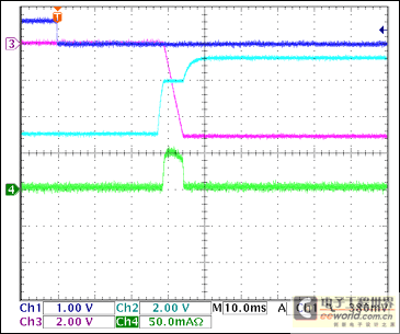
Figure 11. -5V Turn-On Waveforms, No LoadCh1
= Q8BASE, Ch2 = -5VGATE, Ch3 = -5VOUT, Ch4 = IIN(-5V)
Note: IIN(PK) = 55mA, charging the output capacitors.
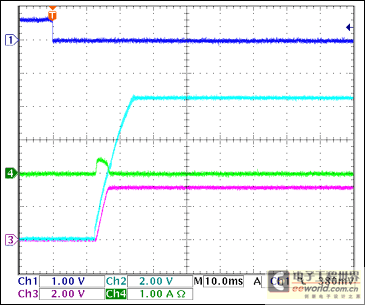
Figure 12. +3.3V Turn-On Waveforms, No LoadCh1
= Q8BASE, Ch2 = +3.3VGATE, Ch3 = +3.3VOUT, Ch4 = IIN(+3.3V)
Note: IIN(PK) = 400mA, charging the output capacitors; +3.3V slew rate is approximately 1V/ms.
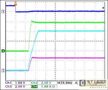
Figure 13. +3.3V Turn-On Waveforms, 1.1Ω Load = 3A
Ch1 = Q8BASE, Ch2 = +3.3VGATE, Ch3 = +3.3VOUT, Ch4 = IIN(+3.3V)
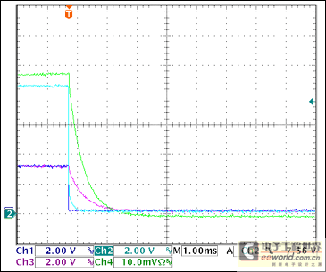
Figure 14. +3.3V Overcurrent ShutdownCh1
= STAT1, Ch2 = VGATE (+3.3V), Ch3 = +3.3VOUT, Ch4 = IOUT(+3.3V) 0.5A/divNote
: The decrease in IOUT and VOUT is due to the output capacitor discharging into the constant resistance load. The measured trigger current is 3.22A. *

Figure 15. +5V Turn-On Load Capacitor Charging Current, No LoadCh1
= Q8BASE, Ch2 = +5VGATE, Ch3 = +5VOUT, Ch4 = IIN(+5V)
Note: IIN(PK) = 500mA, charging the output capacitor.
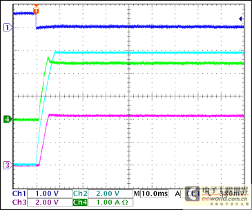
Figure 16. +5V Turn-On Current, 2.083Ω Load = 2.4A
Ch1 = Q8BASE, Ch2 = +5VGATE, Ch3 = +5VOUT, Ch4 = IIN(+5V)
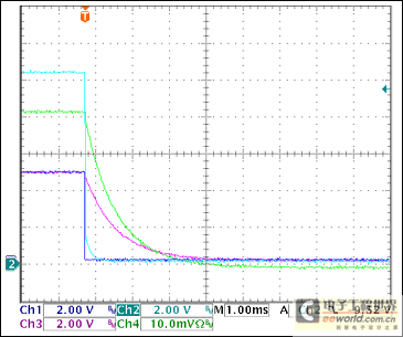
Figure 17. +5V Overcurrent ShutdownCh1
= STAT2, Ch2 = VGATE (+5V), Ch3 = +5VOUT, Ch4 = IOUT(+5V) 0.5A/divNote
: The decrease in IOUT and VOUT is due to the output capacitors discharging into the constant resistance load. The measured trigger current is 2.87A.
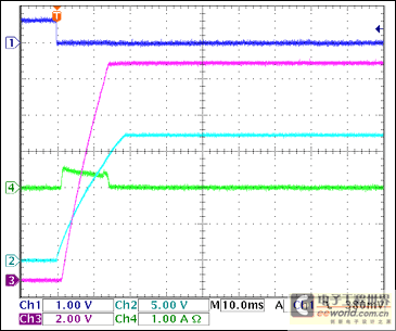
Figure 18. +12V Start-Up Current, No LoadCh1
= Q8BASE, Ch2 = +12VGATE, Ch3 = +12VOUT, Ch4 = IIN(+12V)
Note: IIN(+12Vpk) = 500mA, charging the output capacitors.
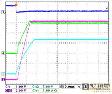
Figure 19. +12V Turn-On Current, 4Ω Load = 3A
Ch1 = Q8BASE, Ch2 = +12VGATE, Ch3 = +12VOUT, Ch4 = IIN(+12V)

Figure 20. +12V Overcurrent ShutdownCh1
= STAT3, Ch2 = VGATE (+12V), Ch3 = +12VOUT, Ch4 = IOUT(+3.3V) 0.5A/divNote
: The decrease in IOUT and VOUT is due to the discharge of the output capacitor into the constant resistance load. The measured trigger current is 3.1A.
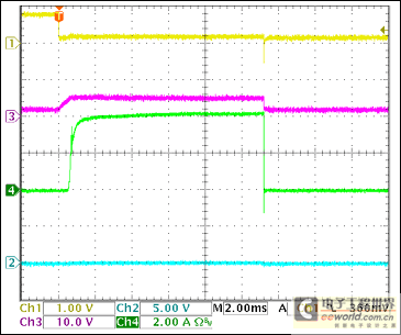
Figure 21. +5V Startup Current for Short Circuit
Ch1 = Q8BASE, Ch2 = +5VOUT, Ch3 = +5VGATE, Ch4 = IIN(+5V)
Note: 4A load current when triggered.

Figure 22. +12V Startup Current for Short Circuit
Ch1 = Q8BASE, Ch2 = VOUT, Ch3 = VGATE, Ch4 =
IOUTNote: 5.7A load current when triggered.
Testing PCB layout
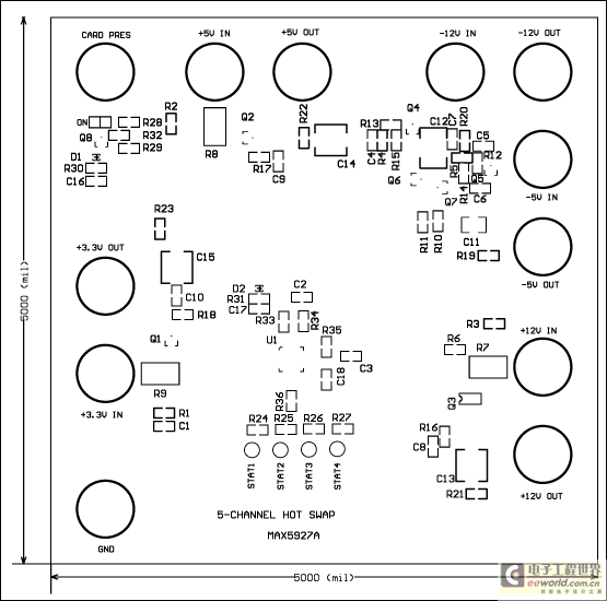
More detailed image (PDF, 237kB)
Figure 23. Reference design PCB component layout
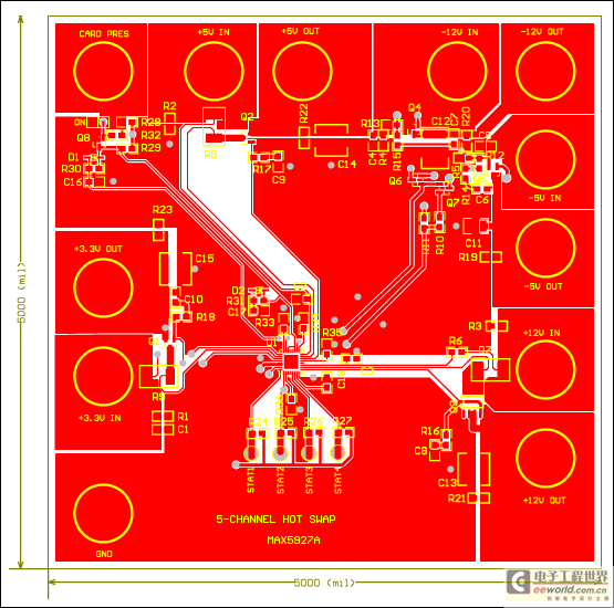
More detailed image (PDF, 330kB)
Figure 24. Top layer

Figure 25. Bottom layer
Materials List
| Qty | Designator | Description | Manufacturer and Part Number |
| 5 | C1, C2, C3, C4, C5 | 1µF ±10%, 25V X7R ceramic capacitors (0805) | — |
| 3 | C6, C7, C18 | 10nF ±10%, 25V X7R ceramic capacitors (0805) | — |
| 1 | C8 | 56nF ±10%, 25V X7R ceramic capacitor (0805) | — |
| 1 | C9 | 68nF ±10%, 25V X7R ceramic capacitor (0805) | — |
| 1 | C10 | 100nF ±10%, 25V X7R ceramic capacitor (0805) | — |
| 1 | C11 | 47µF ±20%, 6.3V X5R electrolytic capacitor (1210) | TDK C3225X5R0J476M |
| 1 | C12 | 100µF +80%, -20%; 16V Y5V ceramic capacitor (2220) | TDK C5750Y5V1C107Z |
| 3 | C13, C14, C15 | 470µF ±20%, 16V electrolytic capacitors | — |
| 1 | C16 | 15nF ±10%, 25V X7R ceramic capacitor (0805) | — |
| 1 | C17 | 33nF ±10%, 25V X7R ceramic capacitor (0805) | — |
| 2 | D1, D2 | 75V, 200mW silicon diodes (SOD-323) | Diodes Inc. MMBD4148WS |
| 2 | Q1, Q2 | 20V, 4.9A, 33mΩ n-channel MOSFETs (SOT23) | Vishay Si2314BDS |
| 1 | Q3 | 30V, 6.9A, 33mΩ n-channel MOSFET (8-SO) | Vishay Si9410BDY |
| 2 | Q4, Q5 | 30V, 4A, 47mΩ n-channel MOSFETs (SOT23) | Vishay Si2306BDS |
| 2 | Q6, Q7 | 60V, 800mA bipolar PNP transistors (SOT23) | Fairchild MMBT2907 |
| 1 | Q8 | 40V, 1A bipolar NPN transistor (SOT23) | Fairchild MMBT2222A |
| 10 | R1, R2, R3, R4, R5, R24, R25, R26, R27, R32 | 100kΩ ±5%, 1/16W thick-film resistors (0805) | — |
| 1 | R6 | 1Ω ±5%, 1/16W thick-film resistor (0805) | — |
| 2 | R7, R9 | 0.008Ω ±1%, 1/4W thick-film resistors (2512) | — |
| 1 | R8 | 0.010Ω ±1%, 1/4W thick-film resistor (2512) | — |
| 2 | R10, R11 | 90.9kΩ ±1%, 1/16W thick-film resistors (0805) | — |
| 2 | R12, R13 | 133kΩ ±1%, 1/16W thick-film resistors (0805) | — |
| 2 | R14, R15 | 15kΩ ±1%, 1/16W thick-film resistors (0805) | — |
| 3 | R16, R17, R18 | 4.7kΩ ±1%, 1/16W thick-film resistors (0603) | — |
| 5 | R19, R20, R21, R22, R23 | 10kΩ ±5%, 1/16W thick-film resistors (0805) | — |
| 1 | R28 | 20kΩ ±5%, 1/16W thick-film resistor (0805) | — |
| 2 | R29, R36 | 100kΩ ±1%, 1/16W thick-film resistors (0805) | — |
| 2 | R30, R31 | 910kΩ ±1%, 1/16W thick-film resistors (0805) | — |
| 2 | R33, R35 | 1.15kΩ ±1%, 1/16W thick-film resistors (0805) | — |
| 1 | R34 | 1.18kΩ ±1%, 1/16W thick-film resistor (0805) | — |
| 1 | U1 | Quad hot-swap controller IC, 32-TQFN-EP | Maxim MAX5927AETJ |
*Note that Figures 14, 17, and 20 use a special current probe that only shows 72% of the true value. The circuit breaker current is measured using an adjustable constant current load, and the point at which it shuts off is marked.
Previous article:Creating Fast Line Transients
Next article:5-channel (3 +V and 2 -V) hot-swap reference design
- Popular Resources
- Popular amplifiers
Latest Analog Electronics Articles
- High signal-to-noise ratio MEMS microphone drives artificial intelligence interaction
- Advantages of using a differential-to-single-ended RF amplifier in a transmit signal chain design
- ON Semiconductor CEO Appears at Munich Electronica Show and Launches Treo Platform
- ON Semiconductor Launches Industry-Leading Analog and Mixed-Signal Platform
- Analog Devices ADAQ7767-1 μModule DAQ Solution for Rapid Development of Precision Data Acquisition Systems Now Available at Mouser
- Domestic high-precision, high-speed ADC chips are on the rise
- Microcontrollers that combine Hi-Fi, intelligence and USB multi-channel features – ushering in a new era of digital audio
- Using capacitive PGA, Naxin Micro launches high-precision multi-channel 24/16-bit Δ-Σ ADC
- Fully Differential Amplifier Provides High Voltage, Low Noise Signals for Precision Data Acquisition Signal Chain
MoreSelected Circuit Diagrams
MorePopular Articles
- Innolux's intelligent steer-by-wire solution makes cars smarter and safer
- 8051 MCU - Parity Check
- How to efficiently balance the sensitivity of tactile sensing interfaces
- What should I do if the servo motor shakes? What causes the servo motor to shake quickly?
- 【Brushless Motor】Analysis of three-phase BLDC motor and sharing of two popular development boards
- Midea Industrial Technology's subsidiaries Clou Electronics and Hekang New Energy jointly appeared at the Munich Battery Energy Storage Exhibition and Solar Energy Exhibition
- Guoxin Sichen | Application of ferroelectric memory PB85RS2MC in power battery management, with a capacity of 2M
- Analysis of common faults of frequency converter
- In a head-on competition with Qualcomm, what kind of cockpit products has Intel come up with?
- Dalian Rongke's all-vanadium liquid flow battery energy storage equipment industrialization project has entered the sprint stage before production
MoreDaily News
- Allegro MicroSystems Introduces Advanced Magnetic and Inductive Position Sensing Solutions at Electronica 2024
- Car key in the left hand, liveness detection radar in the right hand, UWB is imperative for cars!
- After a decade of rapid development, domestic CIS has entered the market
- Aegis Dagger Battery + Thor EM-i Super Hybrid, Geely New Energy has thrown out two "king bombs"
- A brief discussion on functional safety - fault, error, and failure
- In the smart car 2.0 cycle, these core industry chains are facing major opportunities!
- Rambus Launches Industry's First HBM 4 Controller IP: What Are the Technical Details Behind It?
- The United States and Japan are developing new batteries. CATL faces challenges? How should China's new energy battery industry respond?
- Murata launches high-precision 6-axis inertial sensor for automobiles
- Ford patents pre-charge alarm to help save costs and respond to emergencies
Guess you like
- Analog IC Design Resource Download
- The product cannot be connected to the Internet, and the displayed time cannot be updated through the network. The LCD displays the date and time inaccurately. From which angles can it be solved...
- EEWORLD University Hall ---- Top 10 Raspberry Pi Designs in 2019
- Industrial control system software design based on finite state machine.pdf
- CPU and peripherals of TMS320C6000 series DSP
- Design of wireless transmitter for voice, text and short messages
- Overview of air conditioning automatic control system 2
- Realization of Simple Single Chip Microcomputer Calculator
- See how many PA posts have been viewed in the forum
- 【PLC based on IoT】---Testing RPI-400 performance based on AI

 ISL28207FRTZ-T7


 京公网安备 11010802033920号