Low-cost, high-performance digital signal processors (DSPs) with integrated peripherals such as A/D converters (ADCs) and pulse width modulators (PWMs) have been widely used in motor control, uninterruptible power supplies (UPSs), and motion control. Low-cost DSPs provide power designers with new tools for controlling power conversion functions.
Compared with traditional analog control, DSP controllers have many outstanding advantages, such as multi-platform standard hardware design, low sensitivity to aging and environmental changes, excellent noise immunity, easy implementation of advanced control algorithms, flexibility in design changes, and single-chip solution for control and communication functions. However, the use of DSP in power supply design poses new challenges to many analog designers, who must try their best to change their designs to adapt to the new digital environment.
This article uses an average current-mode power factor correction (PFC) boost converter controlled by a Texas Instruments TMS320LF2407A 16-bit fixed-point DSP as an example to illustrate the differences from traditional analog design solutions. Different control loop parameters in the analog control field must be redefined to their digital implementations, and then loop analysis is performed, and the required voltage and current loop compensators are given. Finally, the discreteness of these compensators and their implementation in software are introduced. By taking the PFC-level digital controller design as an example, the basic differences between analog and digital control can be identified.
2. PFC stage circuit controlled by TMS320LF2407A
Figure 1 shows the PFC stage controlled by the TMS320LF2407A. This topology is an AC-DC boost converter that requires three signals to execute the control algorithm, namely the rectified input voltage Vin, the inductor current Iin, and the DC bus (output capacitor Co) voltage V.
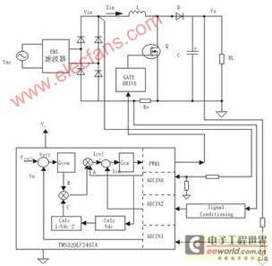
Figure 1 PFC stage circuit controlled by TMS320LF2407A
The converter is controlled by two feedback loops: the average output voltage is regulated by the slower responding outer loop, while the inner loop that shapes the input current responds much faster than the outer loop. The instantaneous signals Vin, Iin and Vo are detected by their respective voltage and current sensing circuits, and the detection signals are fed back to the DSP via three digital-to-analog converter (ADC) channels. The three ADC channels are ADC/NO, ADCIN1 and ADCIN2. The rates of these signals are sensed and converted using the sampling frequency fs of the ADC control loop. The digitally sensed bus voltage Vo is compared with the desired reference bus voltage Vref, and the differential signal (Vref-Vo) is then fed to the voltage loop controller Gvea. The output "B" of the digital controller Gvea is multiplied by the other two signals "A" and "C" to generate the reference current command for the inner current loop. In Figure 1, "A" represents the sensed digital instantaneous signal Vin. "C" can be determined by the following formula:

Wherein, Vdc is the calculated average component of the sensed digitized signal Vin. In Figure 1, Iref is the reference current command of the inner current loop. Iref has a rectified sine wave shape, and its amplitude is sufficient to keep the output voltage at a reference level Vref for changes in load and AC line voltage. The sensed digitized inductor current Iin is compared with the reference current Iref, and the difference between Iref and Iin enters the current controller Gca. The output of Gca finally generates a PWM duty cycle command for the PFC switch.
3. PFC-level digital controller design
The block diagram of the DSP-controlled PFC converter control loop shown in Figure 1 is shown in Figure 2. In the figure, the Kf, Ks and Kd gain blocks replace the previous respective voltage and current sensing and regulation circuits. The multiplier gain Km is also added to the control unit. Km allows the reference signal Iref to be adjusted according to the converter input operating voltage range. The internal current loop is programmed with Iref, and the current loop power stage input duty cycle command is the inductor current Iin. The current controller Gca generates an appropriate control output Uca, causing Iin to follow Iref. The voltage controller Gvea outputs Unv to the voltage loop power stage, and its output is the bus voltage Vo. Gvea generates an appropriate Unv to control the amplitude of Iref so that Vo remains at the reference level. The TMS320LF2407A produced by Texas Instruments (TI) is a 16-bit fixed-point DSP controller that is used to control a universal input (85~265Vac) average current mode PFC pre-converter.
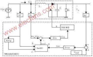
Figure 2 Block diagram of the PFC stage control loop controlled by TMS320LF2407A
3.1 Voltage and Current Sensing Gains
The input voltage Vin and the input current Iin are expressed as
Vin=Vm Sin2wt 0≤Vm≤Vmax
Iin=Im sin2wt 0≤Im≤Imax
respectively
, where: Vmax is the maximum value of the peak amplitude Vm, V; Imax is the maximum value of the peak amplitude Im, A.
DSP-Based PFC Converter The signals are sensed by the on-chip A/D converter. To bring these signals into the range of the A/D converter, appropriate external conditioning circuits are applied to each channel. The user software reads the transformed signals, i.e., the digitized signals. The digitized signals read from the ADC result registers are stored in a temporary memory location using an appropriate fixed-point format. The digitized signals are represented as numerical values using a finite word length. In a 16-bit DSP, the least significant bit (LSB) is used to represent the mantissa of the signal and the most significant bit (MSB) is used to represent its sign. To achieve the conversion, it is necessary to select the range of the signal and then mark the entire range of the result of the change within the entire range of the fixed-point representation. For the TMS320LF2407A DSP, the range of the forward signal is from 0 to 32767. Once this mapping is completed, the next step is to select the appropriate fixed-point arithmetic notation for these digitized signals. For a 16-bit DSP, it is advantageous to use the Q15 notation as the fixed-point representation for these signals. With this representation, the numerical values are within the range of 0 to 32767, representing absolute values between 0 and 1. With the Q15 counting method, voltage and current are automatically saved as normalized per unit (pu) values relative to their maximum values.
In Figure 2, the feedforward voltage sensing gain Kf, current sensing gain Ks and PFC output DC bus voltage sensing gain Kd are expressed as follows:
Kf=1/Vmax
Ks=1/Imax
Kd=1/Vo(max)
Wherein, Vmax is the maximum allowable amplitude of the rectified input voltage Vin, V; Imax is the maximum allowable amplitude of the input current Iin, A; Vo(max) is the maximum allowable value of the DC bus voltage, V.
3.2 Implementation of input voltage feedforward software
Input voltage feed-forward can keep the input power at a specified level regardless of AC line voltage fluctuations.
To calculate the average component Vdc of the input voltage Vin, it is necessary to calculate the signal frequency f (=1/t) and then integrate the signal over one cycle, as described in the diagram of FIG3 .
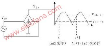
Figure 3 Calculation of the average component of and Vin
3.2.1 Frequency calculation
During and after the frequency software is executed, the number of samples (N) of Vin is counted and saved each time the signal crosses the upper threshold Uth-hi. The lower threshold of the signal Uth-Io is used to obtain the noise immunity. If the sampling period is Ts, the sampling frequency is fs=1/Ts. The period of Vin is T, and N=T/Ts. If N is a known number, the frequency per unit (Pu) fpu is calculated as:

Where fmax is the maximum frequency of Uin, Hz; Nmin is the minimum number of samples over one period of Uin. The user software that calculates the frequency uses the value of N to first calculate the intermediate value 1/N and then multiply it by Nmin to obtain the value of fpu. In order to save the 1/N value with the highest accuracy and without causing the accumulator to overflow, it is important to know the value of Nmin. For this purpose, the user should select the maximum frequency of the signal to be measured. Once the value of Nmin is known, the 1/N quantity can be saved with the highest accuracy and in an appropriate fixed-point representation. For example, for a PFC converter with an input operating frequency of 47~63Hz, the maximum input frequency can be selected as 70Hz. It is then very easy to calculate Nmin using fmax=140Hz (twice the input frequency) and a known Ts value.
3.2.2 Feedforward Component Calculation
As long as the frequency of signal Vin is known, its average component Vdc can be calculated using the following formula:

where T is the time period corresponding to the frequency f of Uin, S; Vin (i) is the digitized i-th sample of Vin.
Since Vin is measured as a per-unit (pu) normalized value relative to its maximum value Vmax, the calculated Vdc value is also a per-unit (pu) value with a Vmax normalized base value. For a sine wave input voltage, the maximum value of Vac is only 2Vmax/π. Therefore, in the fixed point representation of Vac, for best accuracy, the previously calculated value is converted to a per-unit normalized value relative to its own maximum value, which is given by: The

inverse voltage Vinv of Vdc1 (i.e., Vinv=1/Vdc1) is maximum when Vdc1 is minimum and vice versa. To obtain higher accuracy in the fixed point representation of Vinv, it is necessary to represent it with a per-unit (pu) normalized value relative to its maximum value. For a sine wave input voltage, the minimum value of Vdc is 2Vmin/π. The selection of the input voltage minimum amplitude Vmin is based on the input voltage range of the PFC converter. For example: if the low line RMS voltage of the PFC converter is 90V, the Vmin value should be less than or equal to 127V ( ). The maximum value of Vinv is (Vminπ/2), and the per unit (pu) value of the corresponding Vinv relative to its own maximum value is:

3.3 Multiplier gain Km
The multiplier gain Km should be adjusted so that the reference current Iref is at its maximum value at the lowest input voltage when the PFC converter delivers the maximum load. In Figure 2, Iref is With the

current loop closed, Iref can be expressed as

At the lowest operating voltage Vinv=1, the voltage controller output at full load will be at its maximum value, that is, Vnv=1. Therefore, at the lowest operating voltage, in order to produce the maximum reference current, the required Km value is:

3.4 Voltage and current loop compensator
The high frequency approximation of the current loop power stage is:

According to the PFC control block diagram shown in Figure 2, the current loop gain equation is:

Where Fm is the modulator gain,

The modulator is implemented partly in software and partly using the DSP PWM hardware. The software uses the modulator input, i.e. the current controller output Uca, to calculate the duty cycle value for the PWM hardware module in the TMS320LF2407A. The PWM hardware uses the duty cycle value to generate the appropriate PWM signal for the PFC switch. When the modulator input Uca is 1, the software ensures that the modulator output, i.e. the PWM duty cycle, is 100%. In this case, the modulator gain Fm=1. Therefore, for the crossover frequency fci of the current loop, the required current error amplifier compensator can be expressed as:

As long as the current loop is closed, the voltage loop power stage transfer function can be calculated as follows:

Where Zf is the equivalent impedance of the parallel branch consisting of the output capacitor CO and the load impedance ZO, Zf=ZO/(1+sCOZO); load impedance
 .
.
The voltage loop gain equation in Figure 2 is as follows:

The voltage loop crossover frequency fcv requires a voltage error amplifier compensator of

3.5 Implementation of voltage and current loop compensator software
The voltage and current loop controllers given previously are transformed into equivalent digital forms as described below before they are implemented in software using TMS320LF2407A. The current controller can be written as:

Where: KP is the calculated current compensator value; E is the current error signal.
The current loop compensation Bode curve is shown in Figure 4. Among them: the top is the current loop control unit gain Gid, Fm and KS curve; the middle is the compensator Gca gain curve; the bottom is the desired loop gain Ti curve. The power stage has a slope of -1, and placing the zero point fz at the desired crossover frequency fci can produce a 45° phase margin. However, due to the control loop sampling and compensation delay, part of the phase margin is lost, so fz is placed at the position indicated in Figure 4 to compensate for the loss of phase margin.
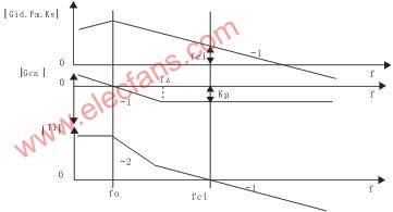
Figure 4 Current loop compensation Bode curve
4. PFC-level digital controller design example
The system parameters in this design are as follows:
Output power PO=825W, DC bus voltage VO=380V, switching frequency fSW=120KHz, digital loop frequency fS=60KHz, L=100μH, C=390μF, fCV=10Hz, fci=8KHz, input voltage maximum frequency fmax=200Hz, Vmax=410V, Vmin=109.95V, Vo(max)=410V, input current maximum value Imax=2PO/Vmin=15A.
The various gain parameters are: kf=1/410, kd=1/410, KS=1/15, Km=410/109.95=3.7286.
4.1 Current Controller Implementation Example
Since fci=8KHz, the current controller value is

Set the current loop PI compensator zero point at 800Hz, and the integral time constant of the current compensator is TIC=1/2π×800=198.94×10-6. Therefore, the complete current loop controller is

Where: KPi=0.1985, Kli=997.77.
The discrete controller execution equation is
Ui(n)=K0i?Ei(n)+li(n-1);
li(n)=li(n-1)+K1i?Ei(n)+Kcorri?Epii
Epii=Usi-Ui(n)
Where: When
 In other cases,
the current controller correlation coefficient is
 .
.
The current controller correlation coefficient is
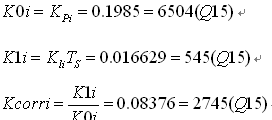
The code snippet executed by the controller is as follows:
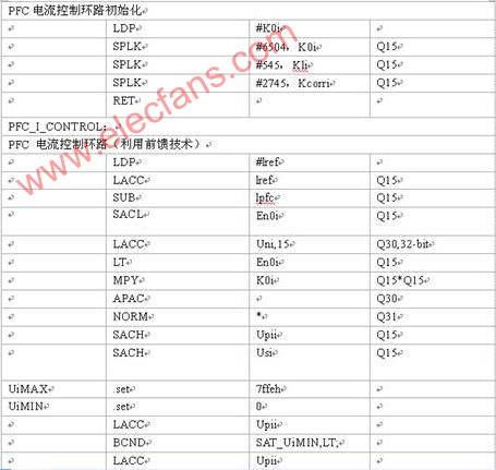
4.2 Voltage Controller Implementation Example
The load impedance of the PFC converter is: .
Since fCV=10Hz, the voltage controller value is GVEA=4.7517.
The voltage loop PI compensator zero point is set at 10Hz, and the integral time constant is: T1V=1/2π×10=15.9155×10-3. Therefore, the complete voltage loop controller is In

the formula, KPV=4.7517, KIV =298.56.
The controller performs the following equations:
Uv(n)=K0v?Ev(n)+Iv(n-1)
Ivi(n)=Iv(n-1)+K1v?Ev(n)+Kcorrv?Epiv
Epiv=Usv-Uv(n)
In the formula, when

the correlation coefficient of the voltage controller is

In the formula
 .
.
The execution code segment of the voltage controller is written in the same way as the current controller.
4.3 Experimental Results
The input current waveform of the PFC converter at an input voltage of 224Vrms is shown in Figure 5(a), and the input current waveform at an input voltage of 100Vrms is shown in Figure 5(b). It can be seen from the input current waveform that its shape tends to be a standard sine wave and is in phase with the input voltage, thus achieving power factor correction.
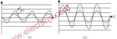
Figure 5 Input current and voltage waveforms (a) 224V input; (b) 100V input
5. Conclusion
The design of PFC converter using DSP is different from the traditional analog control design scheme. Different control loop parameters must be redefined from analog control to their digital implementation. Many engineers with analog control experience face new challenges in adapting to the transition from analog to digital environment.
Previous article:Causes and countermeasures of inverter overvoltage
Next article:Triple Output LED Driver Drives Common Anode LED Strings
- Popular Resources
- Popular amplifiers
- High signal-to-noise ratio MEMS microphone drives artificial intelligence interaction
- Advantages of using a differential-to-single-ended RF amplifier in a transmit signal chain design
- ON Semiconductor CEO Appears at Munich Electronica Show and Launches Treo Platform
- ON Semiconductor Launches Industry-Leading Analog and Mixed-Signal Platform
- Analog Devices ADAQ7767-1 μModule DAQ Solution for Rapid Development of Precision Data Acquisition Systems Now Available at Mouser
- Domestic high-precision, high-speed ADC chips are on the rise
- Microcontrollers that combine Hi-Fi, intelligence and USB multi-channel features – ushering in a new era of digital audio
- Using capacitive PGA, Naxin Micro launches high-precision multi-channel 24/16-bit Δ-Σ ADC
- Fully Differential Amplifier Provides High Voltage, Low Noise Signals for Precision Data Acquisition Signal Chain
- Innolux's intelligent steer-by-wire solution makes cars smarter and safer
- 8051 MCU - Parity Check
- How to efficiently balance the sensitivity of tactile sensing interfaces
- What should I do if the servo motor shakes? What causes the servo motor to shake quickly?
- 【Brushless Motor】Analysis of three-phase BLDC motor and sharing of two popular development boards
- Midea Industrial Technology's subsidiaries Clou Electronics and Hekang New Energy jointly appeared at the Munich Battery Energy Storage Exhibition and Solar Energy Exhibition
- Guoxin Sichen | Application of ferroelectric memory PB85RS2MC in power battery management, with a capacity of 2M
- Analysis of common faults of frequency converter
- In a head-on competition with Qualcomm, what kind of cockpit products has Intel come up with?
- Dalian Rongke's all-vanadium liquid flow battery energy storage equipment industrialization project has entered the sprint stage before production
- Allegro MicroSystems Introduces Advanced Magnetic and Inductive Position Sensing Solutions at Electronica 2024
- Car key in the left hand, liveness detection radar in the right hand, UWB is imperative for cars!
- After a decade of rapid development, domestic CIS has entered the market
- Aegis Dagger Battery + Thor EM-i Super Hybrid, Geely New Energy has thrown out two "king bombs"
- A brief discussion on functional safety - fault, error, and failure
- In the smart car 2.0 cycle, these core industry chains are facing major opportunities!
- The United States and Japan are developing new batteries. CATL faces challenges? How should China's new energy battery industry respond?
- Murata launches high-precision 6-axis inertial sensor for automobiles
- Ford patents pre-charge alarm to help save costs and respond to emergencies
- New real-time microcontroller system from Texas Instruments enables smarter processing in automotive and industrial applications
- I still don't understand the problem of using PNP npn as a switch. 8050 is used as a switch and it keeps turning on and off.
- Msp430 learning notes interrupt processing function
- "It's OK as long as it works, what else do you need?" ST Industry Summit 2019 answer sheet completed and sent a mouse disassembly diagram
- Smart electric car seesaw
- Ultrasonic drive circuit
- Help: How many lines are needed for SWD debugging of stm32f407?
- How to use STM32 to read Windows vector fonts
- Recruiting part-time DSP and other related professional lecturers or technical support personnel
- [CC1352P Review] TI-RTOS uartecho test
- [Erha Image Recognition Artificial Intelligence Vision Sensor] Use serial communication to conduct in-depth communication and data analysis with Erha Dog

 LM121H/883B


 京公网安备 11010802033920号