|
 At present, developed countries have increasingly stringent requirements on
the power consumption of
electrical
appliances and have formulated many standard specifications for standby power consumption. In order to meet these specifications, many new technologies have emerged. The main idea is to allow
the switching
power supply
to operate at a lower
switching
frequency
when the load is very small or no-load in standby mode
. This article discusses three more commonly used frequency reduction technologies, namely pulse skipping, burst mode and off time modulation, and introduces how to reduce the switching frequency to achieve the purpose of reducing standby power consumption.
In
the green era where
environmental
awareness is increasingly valued, the effective use of limited
energy
has become a consensus among people. European and American countries have defined clear specifications for the power consumption of electrical products in no-load standby mode. The specific regulations published by the European Union (EEC) are shown in Table 1. In the United States, since July 2001, the country has stipulated that government agencies are not allowed to purchase electrical products with standby power consumption exceeding 1W.
 It can be seen that in the near future, low standby power consumption of power converters will become a basic requirement, which is also a challenge that power supply design engineers must face.
Switching power supply loss analysis
The loss of a switching power supply includes conduction loss, switching loss, and peripheral
control
circuit
loss.
The causes of loss in different parts of
the circuit
are different, so the methods of suppressing loss are also different. It is necessary to quantify these losses with mathematical equations, and then sort out the methods to reduce the losses of each part, so as to come up with a specific and effective solution to reduce the overall loss. For the convenience of discussion, this article takes the commonly used flyback converter as an example, expresses the losses of each part with mathematical equations, and lists the solutions. Table 2, Table 3 and Table 4 are
the causes and solutions of
conduction loss, switching loss and peripheral
control
circuit loss respectively.
It is obvious from the analysis results of these tables that the conduction loss and switching loss are closely related to the switching frequency of the converter, and a higher frequency can reduce the converter's requirements for the size of energy storage components (inductors and
capacitors
). In order to reduce the loss of the converter when it is in standby mode, the switching frequency of the converter is reduced when it is low load or no load, which can take into account both the component volume and energy loss. At present, many technologies have been applied to actual power management ICs based on this concept. Below we will introduce the design concepts and characteristics of three of the more widely used technologies.
Pulse skipping technology
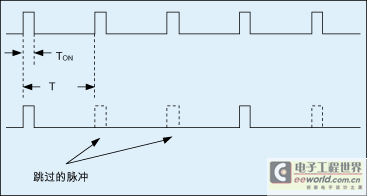
Figure 1 is a schematic diagram of pulse skipping technology. When the load is reduced,
the switching pulses
driving
the power switch will be masked (i.e. skipped). The omission of some pulses is equivalent to reducing the switching frequency, which can reduce the loss caused by high-frequency switching. However, this frequency reduction method will cause the output voltage to drop or rise suddenly (Figure 2).

In a flyback converter, energy is stored in the transformer magnetizing inductance when the primary switch is turned on. When the switch is turned off, the previously stored energy is released to the load. The power stored in the magnetizing inductance can be expressed as
(f
S
×V
in
2
×T
ON
2
)/(2×L
P
). When the load is reduced to a certain extent, the pulse skipping mechanism will halve the effective switching frequency, which means that the power supplied by the converter to the load is halved. Therefore, the flyback circuit will increase the pulse width to make up for the power required by the output load. Before the pulse width increases to the power required by the load, the output voltage will drop suddenly. The opposite situation occurs when the equivalent switching frequency increases, and the output voltage will rise suddenly. This sudden increase and decrease in output voltage during load changes is the inevitable result of discontinuous changes in switching frequency (increase or decrease by integer multiples).

Mutation Mode
The sudden mode technology is also called hiccup mode or cycle skipping mode (Figure 3). Under heavy load conditions, the flyback circuit modulates the pulse width according to the output voltage change. When the load is reduced to a certain level, the control circuit will maintain the original pulse width and periodically skip some pulses. The control circuit reduces the total pulse width or increases the length of the blanking cycle to achieve the purpose of reducing losses. This technology has two obvious disadvantages, namely, low-frequency interference will appear together with the blanking cycle, and sudden changes in load will also cause a sudden drop in the output voltage.


Off-time modulation technology
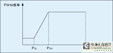
Figure 4 shows the basic principle of non-conduction time modulation. When the load changes, the switching frequency will continuously decrease or increase, and the relationship between the switching frequency and the output power is shown in Figure 5. In addition to effectively reducing energy loss, this method of continuously modulating the switching frequency when the load is low or no load can also avoid the problem of sudden increase or decrease in output voltage in the first two methods.
Starting circuit loss


The loss of the starting circuit accounts for a high proportion of the no-load standby loss of the power converter. Here we introduce a starting circuit with fast starting speed and low loss. Figure 6(a) is a traditional starting circuit, where VSTA is the starting critical voltage of the pulse width modulation controller, T
D_ON
is the starting delay time, and T
D_ON
= (C1×VSTA)/IC1. Using a larger input
resistor
(Rin) can effectively reduce
the resistance
loss, but the starting delay time will be extended. Therefore, it is recommended to use the circuit of Figure 6(b), where the capacitor C1 is smaller, so that the loss of the starting circuit can be reduced when a large input resistor is used, while still having a faster starting speed. The larger capacitor C2 can provide a stable voltage for the controller to use without increasing the starting delay time.

Figure 7 shows an AC-DC converter with an input voltage of 90 to 264 Vrms and an output of 12 V/5 A. The control chip used is SG6841, which adopts BiCMOS technology. Its non-conduction time modulation starts to work when the load drops to 20%, and the input resistance is 3 MΩ. Table 5 lists the main measurement results. Under no-load conditions, the switching frequency is designed between 2 and 8 KHz to reduce audio interference.
Related links
Next-generation
mobile
phones: Power management challenges and design trends
http://www.eetchina.com/ART_8800319906.HTM
How to test the power supply ripple and output noise
http://www.eetchina.com/ART_8800314288.HTM
Use hardware and firmware to reduce
power consumption in
battery-
powered products
http://www.eetchina.com/ART_8800311350.HTM
References

[1]. R. Erickson, D. Maksimovic, Fundamentals of Power Electronics, 2nd ed., 2001 Kluwer Academic publishers.
[2]. Sandri, et al., "DC-to-DC converter functioning in a pulse slipping mode with low power consumption and PWM inhibit," US patent 5,745,352, Api. 1998, SGS-Thompson.
[3]. Culpepper, et al., "Switching DC-to-DC converter with discontinuous pulse skipping and continuous operating mode without external sense resistor," US patent 6,396,252, May 2002, National Semiconductor.
[4]. Majid et al., "Low power stand-by for switched-mode power supply circuit with burst mode operation," US patent 5,812,383, Sep. 1998, Philips Electronics.

[5]. T. Yang, "Pulse width modulation controller having frequency modulation for power converter," US patent 09/931,641, System General Inc.
[6]. T. Yang, "PWM controller having off-time modulation for power converter," US patent 6,545,882, Aug 2001, System General Inc
[7]. T. Yang, et al., "PWM controller having adaptive off-time modulation for power saving," US patent pending 10/065,531, System General Inc.
|

 At present, developed countries have increasingly stringent requirements on
the power consumption of
electrical
appliances and have formulated many standard specifications for standby power consumption. In order to meet these specifications, many new technologies have emerged. The main idea is to allow
the switching
power supply
to operate at a lower
switching
frequency
when the load is very small or no-load in standby mode
. This article discusses three more commonly used frequency reduction technologies, namely pulse skipping, burst mode and off time modulation, and introduces how to reduce the switching frequency to achieve the purpose of reducing standby power consumption.
 It can be seen that in the near future, low standby power consumption of power converters will become a b


 LM741ECN


 京公网安备 11010802033920号