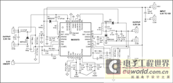
This article presents a detailed reference design using the MAX5073 dual-channel step-down converter operating at a switching frequency of 2MHz. This design can be used in
applications where
board
space is limited, as the higher switching frequency allows for smaller passive components. In addition, this
power
solution can be used in automotive
electronics
(with load dump protection), i.e., products that require switching frequencies outside the AM frequency modulation band. For example, automotive instrument clusters and infotainment systems.
The key specifications of the reference design are listed below, along with a detailed schematic (Figure 1) and bill of materials (Table 1) required for the application.

Details Schematic (PDF)
Figure 1. MAX5073 Reference Design
Table 1. Bill of Materials
The data obtained from the actual measurement circuit gives the efficiency indicators of the device. For details, see Table 2 and Table 3.
Table 2. Efficiency indicators when VOUT2 is disabled
fSW = 2MHz, LOUT = 4.7µH, COUT = 22µF/6.3V (ceramic capacitor )
Table 3. Efficiency Specifications with VOUT1 Disabled
fSW = 2MHz, LOUT = 4.7µH, COUT = 22µF/6.3V (Ceramic Capacitor)
In terms of stability, Figures 2 and 3 show the Bode plots for each output, detailing the gain and phase of each output.

Figure 2. 3.3V/1.4A VOUTPUT Bode Plot

Figure 3. 2.5V/0.6A VOUTPUT Bode Plot
Reference address:Reference Design of the MAX5073 Dual-Channel Step-Down Converter Operating at 2MHz Switching Frequency
The key specifications of the reference design are listed below, along with a detailed schematic (Figure 1) and bill of materials (Table 1) required for the application.
Specification
- Input voltage: 5.5V to 16V
- Converter 1 output voltage = 3.3V/2A (max)
- Converter 2 output voltage = 2.5V/1A (max)
- Switching frequency of each converter (fSW) = 2MHz
- Ambient Temperature (TA) = -40°C to +85°C

Details Schematic (PDF)
Figure 1. MAX5073 Reference Design
Table 1. Bill of Materials
| Designator | Value | Description | Part | Footprint | Manufacturer | Quantity |
| C1 | 100µF/35V | Capacitor | EEVFK1V101P | 8mm x 10.2mm | Panasonic | 1 |
| C2, C3, C4, C17, C18 | 0.1µF/25V | Capacitors | GRM188R71E104KA01D | 603 | Murata | 5 |
| C5, C6, C7 | 22µF/6.3V | Capacitors | GRM31CR60J226KE19 | 1206 | Murata | 2 |
| C8, C9 | 10µF/25V | Capacitors | GRM31CR61E106KA12 | 1206 | Murata | 1 |
| C10, C12 | 2.2nF | Capacitors | GRM188R71H222JA01 | 603 | Murata | 2 |
| C11 | 560pF | Capacitor | GRM188R71H561KA01 | 603 | Murata | 1 |
| C13, C14 | 22pF | Capacitors | GRM1885C1H220JA01 | 603 | Murata | 2 |
| C15 | 1nF | Capacitor | GRM18871H102KA01 | 603 | Murata | 1 |
| C16 | 4.7µF/6.3V | Capacitor | GRM188R60J475KE19B | 603 | Murata | 1 |
| C19 | 0.22µF/10V | Capacitor | GRM188R71A224KA01 | 603 | Murata | 1 |
| C20 | 0.01µF | Capacitor | GRM188R71H103KA01J | 603 | Murata | 1 |
| D1, D2 | 30V, 500mA | Schottky diodes | MBR0530 | SOD123 | ON Semiconductor | 2 |
| D3 | 40V, 3A | Schottky diode | MBRS340 | SMC | ON Semiconductor | 1 |
| D4 | 40V, 2A | Schottky diode | MBRS240 | SMB | ON Semiconductor | 1 |
| L1, L2 | 4.7µH | Inductors | IHLP2525-CZ | 6.86mm x 6.47mm x 3.18mm | Vishay | 1 |
| R1, R11 | 100kΩ | Resistors | SMD, 1%, 0.125W | 603 | Vishay | 2 |
| R2 | 6.8Ω | Resistor | SMD, 1%, 0.125W | 603 | Vishay | 1 |
| R3 | 4.7Ω | Resistor | SMD, 1%, 0.125W | 603 | Vishay | 1 |
| R4, R8, R10 | 1.18kΩ | Resistors | SMD, 1%, 0.125W | 603 | Vishay | 3 |
| R5, R9 | 27.4kΩ | Resistors | SMD, 1%, 0.125W | 603 | Vishay | 2 |
| R6 | 10kΩ | Resistor | SMD, 1%, 0.125W | 603 | Vishay | 1 |
| R7 | 12.7 kΩ | Resistor | SMD, 1%, 0.125W | 603 | Vishay | 1 |
| R12 | 2.2Ω | Resistor | SMD, 1%, 0.125W | 603 | Vishay | 1 |
| R13 | 6.19kΩ | Resistor | SMD, 1%, 0.125W | 603 | Vishay | 1 |
| R14 | 8.76kΩ | Resistor | SMD, 1%, 0.125W | 603 | Vishay | 1 |
| U1 | MAX5073 | Dual buck converter | MAX5073ETI+ | 32-TQFN_EP (5mm x 5mm) | Maxim | 1 |
The data obtained from the actual measurement circuit gives the efficiency indicators of the device. For details, see Table 2 and Table 3.
Table 2. Efficiency indicators when VOUT2 is disabled
fSW = 2MHz, LOUT = 4.7µH, COUT = 22µF/6.3V (ceramic capacitor )
| VIN (V) | IIN (A) | VOUT1 (V) | IOUT1 (A) | Efficiency (%) |
| 14.007 | 0.065732 | 3.3371 | 0.1018 | 36.8973371 |
| 14.010 | 0.183690 | 3.3339 | 0.5122 | 66.3542117 |
| 14.005 | 0.267750 | 3.3321 | 0.8032 | 71.3722082 |
| 14.007 | 0.329490 | 3.3309 | 1.0112 | 72.9812485 |
| 14.005 | 0.449290 | 3.3298 | 1.4007 | 74.1230723 |
| 14.002 | 0.584520 | 3.3281 | 1.8203 | 74.0201375 |
| 14.001 | 0.650260 | 3.3267 | 2.0150 | 73.6279304 |
Table 3. Efficiency Specifications with VOUT1 Disabled
fSW = 2MHz, LOUT = 4.7µH, COUT = 22µF/6.3V (Ceramic Capacitor)
| VIN (V) | IIN (A) | VOUT2 (V) | IOUT2 (A) | Efficiency (%) |
| 14.008 | 0.044533 | 2.5350 | 0.1075 | 43.6845979 |
| 14.008 | 0.067144 | 2.5337 | 0.2049 | 55.1967881 |
| 14.003 | 0.087638 | 2.5337 | 0.3010 | 62.1452787 |
| 14.004 | 0.109076 | 2.5337 | 0.4003 | 66.3986847 |
| 14.005 | 0.133680 | 2.5337 | 0.5122 | 69.3178710 |
| 14.005 | 0.155350 | 2.5338 | 0.6097 | 71.0058542 |
| 14.008 | 0.255976 | 2.5334 | 1.0001 | 70.6597037 |
In terms of stability, Figures 2 and 3 show the Bode plots for each output, detailing the gain and phase of each output.

Figure 2. 3.3V/1.4A VOUTPUT Bode Plot

Figure 3. 2.5V/0.6A VOUTPUT Bode Plot
Previous article:RS-422 Repeater with less than 3µA Standby Current
Next article:Harmonic Control of Single-Phase Square Wave Inverter Circuit
- Popular Resources
- Popular amplifiers
Latest Analog Electronics Articles
- High signal-to-noise ratio MEMS microphone drives artificial intelligence interaction
- Advantages of using a differential-to-single-ended RF amplifier in a transmit signal chain design
- ON Semiconductor CEO Appears at Munich Electronica Show and Launches Treo Platform
- ON Semiconductor Launches Industry-Leading Analog and Mixed-Signal Platform
- Analog Devices ADAQ7767-1 μModule DAQ Solution for Rapid Development of Precision Data Acquisition Systems Now Available at Mouser
- Domestic high-precision, high-speed ADC chips are on the rise
- Microcontrollers that combine Hi-Fi, intelligence and USB multi-channel features – ushering in a new era of digital audio
- Using capacitive PGA, Naxin Micro launches high-precision multi-channel 24/16-bit Δ-Σ ADC
- Fully Differential Amplifier Provides High Voltage, Low Noise Signals for Precision Data Acquisition Signal Chain
MoreSelected Circuit Diagrams
MorePopular Articles
- Innolux's intelligent steer-by-wire solution makes cars smarter and safer
- 8051 MCU - Parity Check
- How to efficiently balance the sensitivity of tactile sensing interfaces
- What should I do if the servo motor shakes? What causes the servo motor to shake quickly?
- 【Brushless Motor】Analysis of three-phase BLDC motor and sharing of two popular development boards
- Midea Industrial Technology's subsidiaries Clou Electronics and Hekang New Energy jointly appeared at the Munich Battery Energy Storage Exhibition and Solar Energy Exhibition
- Guoxin Sichen | Application of ferroelectric memory PB85RS2MC in power battery management, with a capacity of 2M
- Analysis of common faults of frequency converter
- In a head-on competition with Qualcomm, what kind of cockpit products has Intel come up with?
- Dalian Rongke's all-vanadium liquid flow battery energy storage equipment industrialization project has entered the sprint stage before production
MoreDaily News
- Allegro MicroSystems Introduces Advanced Magnetic and Inductive Position Sensing Solutions at Electronica 2024
- Car key in the left hand, liveness detection radar in the right hand, UWB is imperative for cars!
- After a decade of rapid development, domestic CIS has entered the market
- Aegis Dagger Battery + Thor EM-i Super Hybrid, Geely New Energy has thrown out two "king bombs"
- A brief discussion on functional safety - fault, error, and failure
- In the smart car 2.0 cycle, these core industry chains are facing major opportunities!
- The United States and Japan are developing new batteries. CATL faces challenges? How should China's new energy battery industry respond?
- Murata launches high-precision 6-axis inertial sensor for automobiles
- Ford patents pre-charge alarm to help save costs and respond to emergencies
- New real-time microcontroller system from Texas Instruments enables smarter processing in automotive and industrial applications
Guess you like
- A40i Platform Application Notes - Huawei - ME909S-4G Module Porting Application
- The news about the Agilex M series has been released for some time, but I haven’t seen any information about the specific pin packaging, etc.?
- PIC16F1824
- EEWORLD University ---- Webinar - How to quickly design power rails for Xilinx FPGA and SoC
- EEWORLD University----simulink video tutorial
- Interleaved CCM Totem Pole Bridgeless Power Factor Correction (PFC) Reference Design
- Openmv3 photography
- [2022 Digi-Key Innovation Design Competition] Distributed Temperature and Humidity Acquisition System-STM32H745I-DISCO Basic Learning
- Start at 2pm: TI MSP430 development training, online hands-on demo + analysis by frontline experts
- Chip Manufacturing: A Practical Tutorial on Semiconductor Process Technology (Sixth Edition)

 LF398S8


 京公网安备 11010802033920号