This paper designs a folded common-source common-gate transconductance operational amplifier with a gain enhancement structure and switched capacitor common-mode feedback, which can be used in pipeline A/D. Considering the performance and layout factors, a single-ended amplifier is used as a gain enhancement auxiliary amplifier. And by improving the common-mode negative feedback circuit, the amplifier output common-mode feedback voltage stabilizes faster and has less jitter. This design simulates the circuit and layout of the operational amplifier in the Cadence environment. The results show that the performance parameters of the amplifier have achieved ideal results.
1 Analysis and design of circuit structure
Common structures of CMOS transconductance operational amplifiers include two-stage amplification structure, sleeve structure and folded cascode structure. Although the op amp circuit structure of the two-stage amplification structure has the advantages of high gain and high swing, since at least one pole is introduced in each stage, in order to ensure that the phase-frequency characteristics of the entire amplifier meet the requirements, an additional frequency compensation circuit is required, thereby increasing the current and power consumption of the amplifier, limiting the amplifier bandwidth, and reducing the amplifier speed. Therefore, it cannot meet the requirements for the bandwidth and speed of the op amp in this design. Although the sleeve structure has higher gain, better frequency characteristics and lower power consumption, it is limited by the structure, and its output swing and common-mode input range are small, which does not meet the design requirements. The folded cascode structure improves the disadvantage of the sleeve structure with small output swing. By increasing the number of circuit branches and improving power consumption, it meets the requirements of large bandwidth, high swing and high speed while providing higher gain. By applying gain enhancement technology to the folded cascode structure, the DC gain of the circuit can be further improved without affecting the signal bandwidth, slew rate and phase characteristics. Therefore, in view of the special requirements of this design, a folded cascode structure using gain enhancement technology was selected.
1.1 Main op amp circuit
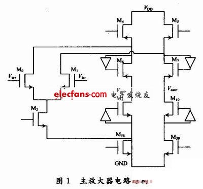
The folded cascode operational amplifier designed in this paper is shown in Figure 1. M0 and M1 are differential input pairs; M2 is a differential pair constant current source; M4 and M5 are current sources; M6 and M7 are common gate tubes; M8, M10, M58, and M59 are common source and common gate current source loads. Since the carrier mobility of NMOS tubes is higher, using NMOS tubes as differential input stages can improve the gain and bandwidth of the operational amplifier.

When there is no gain boost to the auxiliary op amp, the small signal voltage gain of the main op amp is:

It can be seen that compared with the basic constant current source load amplifier circuit, the output resistance of the output node increases by gmRout times, so the operational amplifier with a common source and common gate structure can provide high gain.
1.2 Switched capacitor common mode negative feedback circuit
Since the folded common-source common-gate amplifier requires an extremely precise bias voltage to stabilize the circuit output common mode at a fixed value, a common-mode negative feedback circuit must be introduced to stabilize the output common mode of the entire circuit at the required output voltage common mode. Commonly used common-mode negative feedback circuits are divided into two types: continuous-time common-mode negative feedback and switched capacitor common-mode negative feedback. Since the switched capacitor common-mode negative feedback has no static power consumption and has a small impact on the amplifier itself, the switched capacitor common-mode negative feedback circuit is selected in this design to stabilize the output common mode. Figure 2 is a traditional switched capacitor common-mode feedback circuit, out+, out- are differential output voltage signals, clock1, clock2 are two-phase non-overlapping clock signals, Vcm is a reference voltage for comparison, which is equal to the desired output common-mode voltage; in order to provide a large output swing, half of the power supply voltage is usually taken, Vt is the bias voltage generated by the bias circuit, and Vb1 is the generated adjustment voltage, which is used to stabilize the output common-mode voltage.

Since the switched capacitor common-mode negative feedback needs to continuously calculate the difference between the output common mode and Vcm to control the amplifier so that its output common mode is stable at the required voltage value. For the traditional switched capacitor common-mode negative feedback circuit, half of the clock cycle in a clock cycle requires two capacitors C1 and C2 to take the difference between Vcm and Vt, and cannot be used to interact with the output common mode to generate feedback voltage. Therefore, the common-mode level is slow to establish. Therefore, we introduce another set of sampling capacitors, so that the two sets of sampling capacitors collect the difference between Vcm and Vt, and calculate with the common mode of the output voltage in different clock cycles. In this way, the circuit reduces the establishment time of the common-mode feedback voltage and reduces the jitter of the feedback voltage caused by the switch on and off. The improved common-mode negative feedback circuit is shown in Figure 3.
Since the capacitor in the switch constant capacitance common mode negative feedback circuit is directly connected to the output node, too large a capacitance value will reduce the bandwidth and slew rate of the amplifier. At the same time, in order to reduce the clock feedthrough effect caused by dynamic switching action and other parasitic stray capacitance and back-end process accuracy, the capacitance value cannot be too small. Therefore, in this design, we set all capacitors to 0.5pF.
1.3 Auxiliary amplifier circuit for gain improvement
The use of gain enhancement technology can effectively improve the DC gain of the operational amplifier without affecting its speed. Considering the contribution of layout symmetry to reducing amplifier offset, this design introduces four single-ended current mirror cascode amplifiers as gain-enhancing amplifiers, which are divided into two groups to increase the equivalent resistance from the cascode tube and the equivalent resistance of the cascode current mirror, thereby greatly improving the DC gain. The auxiliary amplifier uses current input, and the current input from the main amplifier circuit to the auxiliary amplifier is determined by the ratio of the input tube size to the corresponding cascode device size. Compared with the traditional differential structure, the single-ended amplifier can be better symmetrically distributed on both sides of the main amplifier layout, and because the amplifier uses a current input that is proportional to the main branch, compared with the voltage input amplifier, it eliminates the impact caused by the input common-mode voltage change. The auxiliary amplifier structure is shown in Figure 4.


Since the auxiliary amplifier has limited output swing and high gain, a common-mode negative feedback structure using differential pair sampling is selected. This structure will limit the amplifier output swing, but will not affect the amplifier gain, and has low power consumption, so it is suitable for use in the auxiliary amplifier. The common-mode negative feedback circuit is shown in Figure 5.
1.4 Bias Circuit
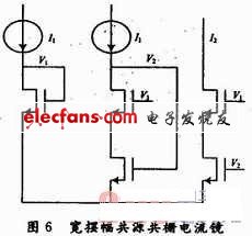
Since there are many cascode tubes in the whole circuit that need to be biased, a wide swing cascode current mirror is used to bias these tubes. The wide swing cascode current mirror increases the swing while ensuring the current replication accuracy, so that the circuit can maintain normal operation while ensuring the output swing. The circuit diagram of the wide swing cascode current mirror is shown in Figure 6, where I2=I1.

2 Circuit Simulation Results
The entire op amp and its bias circuit are designed using SMIC 0.18μm CMOS mixed signal process and simulated using Spectre in the Cadence environment, with a power supply voltage of 3.3V and a load capacitance of 3 pF. The circuit is AC simulated, and the simulation results show that the circuit has a DC gain of 119.3 dB, a unity gain bandwidth of 378.1 MHz, and a phase margin of 60°, as shown in Figure 7.

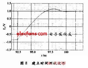
The amplifier takes 7.9 ns to settle to an output voltage with an accuracy of 0.1%. The test waveform is shown in Figure 8.

Common mode input range 600mV~3.3V; voltage output range 0.6~3.1V; power consumption 39mW.
3. Layout Design
The overall circuit includes 1 main amplifier, 2 gainboosts and 1 common mode negative feedback. The main amplifier and gainboost each have their own bias circuit. The bias circuit of gainboost and the gai-nboost amplifier are placed close to each other to make the connection as short as possible. The 2 gainboots are placed on both sides of the main amplifier to make the overall layout symmetrical. The switched capacitor common mode negative feedback is placed under the main amplifier to make the connection between out+, out- and Vb1 as short as possible. The main amplifier is ABAB matched and uses double-sided power supply to ensure better matching of differential mode signals. The bias of the main amplifier is split on both sides of the main amplifier to make the overall layout more regular and neat, saving area.
4 Conclusion
The design of a folded cascode operational amplifier is introduced. The actual design simulation values are: small signal low frequency voltage gain 119.3 dB; unity gain bandwidth 378.1 MHz; phase margin 60°; settling time 7.9 ns; power supply voltage 3.3 V; common mode input range 600 mV~3.3 V; voltage output range 0.6~3.1 V; load capacitance 3 pF; power consumption 39 mW. The whole design meets the design index requirements and is applied to the design of 12 b, 60 MHz pipeline ADC with undersampling technology.
Previous article:Methods to simplify switching power supply design
Next article:The influence of phase detector frequency on the FM linearity of the generated signal
Recommended ReadingLatest update time:2024-11-17 01:32


- Popular Resources
- Popular amplifiers
-
 Operational Amplifier Practical Reference Handbook (Edited by Liu Changsheng, Zhao Mingying, Liu Xu, etc.)
 -
 A Complete Illustrated Guide to Operational Amplifier Applications (Written by Wang Zhenhong)
 -
 Design of isolated error amplifier chip for switching power supply_Zhang Rui
 -
 DAM medium wave transmitter high frequency power amplifier module test platform_Tian Tian
- High signal-to-noise ratio MEMS microphone drives artificial intelligence interaction
- Advantages of using a differential-to-single-ended RF amplifier in a transmit signal chain design
- ON Semiconductor CEO Appears at Munich Electronica Show and Launches Treo Platform
- ON Semiconductor Launches Industry-Leading Analog and Mixed-Signal Platform
- Analog Devices ADAQ7767-1 μModule DAQ Solution for Rapid Development of Precision Data Acquisition Systems Now Available at Mouser
- Domestic high-precision, high-speed ADC chips are on the rise
- Microcontrollers that combine Hi-Fi, intelligence and USB multi-channel features – ushering in a new era of digital audio
- Using capacitive PGA, Naxin Micro launches high-precision multi-channel 24/16-bit Δ-Σ ADC
- Fully Differential Amplifier Provides High Voltage, Low Noise Signals for Precision Data Acquisition Signal Chain
- Innolux's intelligent steer-by-wire solution makes cars smarter and safer
- 8051 MCU - Parity Check
- How to efficiently balance the sensitivity of tactile sensing interfaces
- What should I do if the servo motor shakes? What causes the servo motor to shake quickly?
- 【Brushless Motor】Analysis of three-phase BLDC motor and sharing of two popular development boards
- Midea Industrial Technology's subsidiaries Clou Electronics and Hekang New Energy jointly appeared at the Munich Battery Energy Storage Exhibition and Solar Energy Exhibition
- Guoxin Sichen | Application of ferroelectric memory PB85RS2MC in power battery management, with a capacity of 2M
- Analysis of common faults of frequency converter
- In a head-on competition with Qualcomm, what kind of cockpit products has Intel come up with?
- Dalian Rongke's all-vanadium liquid flow battery energy storage equipment industrialization project has entered the sprint stage before production
- Allegro MicroSystems Introduces Advanced Magnetic and Inductive Position Sensing Solutions at Electronica 2024
- Car key in the left hand, liveness detection radar in the right hand, UWB is imperative for cars!
- After a decade of rapid development, domestic CIS has entered the market
- Aegis Dagger Battery + Thor EM-i Super Hybrid, Geely New Energy has thrown out two "king bombs"
- A brief discussion on functional safety - fault, error, and failure
- In the smart car 2.0 cycle, these core industry chains are facing major opportunities!
- Rambus Launches Industry's First HBM 4 Controller IP: What Are the Technical Details Behind It?
- The United States and Japan are developing new batteries. CATL faces challenges? How should China's new energy battery industry respond?
- Murata launches high-precision 6-axis inertial sensor for automobiles
- Ford patents pre-charge alarm to help save costs and respond to emergencies
- A port to type C port problem
- Build a Prank HID Device with Pico and CircuitPython
- Simulink and UDS on Can
- How to optimize FPGA design area
- TI mmWave sensor carrier card platform
- 51 single chip digital tube serial communication
- Is it possible to use gallium nitride?
- Smoother than oil, make an electric ice pot with hard disk platters and breast pump
- [Third Batch of Shortlist] GigaDevice GD32L233 Review Activity
- [Practice Together in 2021] Looking Back at 2020 and Looking Forward to 2021

 Operational Amplifier Practical Reference Handbook (Edited by Liu Changsheng, Zhao Mingying, Liu Xu, etc.)


 京公网安备 11010802033920号