When using high-speed ADCs (analog-to-digital converters) for product development, or when evaluating these devices for use in a design, it is important to pay attention to the ADC's output harmonics. ADCs typically use differential inputs to minimize common-mode noise and distortion, but these inputs are most effective only when they are balanced and symmetrical. A test system consisting of two RF signal generators and an oscillator can be used to measure the effects of differential imbalance on the ADC input.
When the differential analog inputs of an ADC become unbalanced due to being driven out of phase, even-order distortion increases in the device output. The following describes how to measure the harmonic performance of a high-speed ADC to understand the effects of differential imbalance.
1 Test Setup
The test setup (shown in Figure 1) uses two RF signal generators to drive the ADC analog inputs with a frequency range of 2 MHz to 300 MHz. It is important to lock the reference frequencies of the signal generators to each other to help limit undesired phase drift over time. The output of each signal generator is passed through a low-pass filter that is connected to a two-way low-loss splitter so that the differential signal can be observed with an oscilloscope. The same manufacturer and model of low-loss splitters should be used on each input. In order to use the ADC, an evaluation board is required. In addition, two low-pass filters or band-pass filters of the same manufacturer and model should be used before the splitter to limit broadband noise from the signal generators.
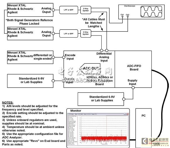
Figure 1. Test setup for measuring phase imbalance.
A consistent analog signal path minimizes measurement errors. The cables before and after the splitter should be the same type and the same length. It is easy to understand that the cable length from the signal generator to the splitter must be the same. The cable length after the splitter (to the ADC and oscilloscope) is easily overlooked and also needs to be the same length to protect the measurement results. If there are traces from the connection point to the ADC pins on the evaluation board, the same length of trace must also be replicated from the splitter to the oscilloscope. Therefore, the cable length from the splitter to the oscilloscope may need to be slightly different to account for the trace differences. Equivalent signal paths ensure that the signal you view on the oscilloscope accurately represents the signal at the ADC analog input pins.
The recommended approach would seem to be to solder the oscilloscope probe leads directly to the analog inputs of the ADC to get the correct length match, but this approach adds parasitic capacitance and inductance to the ADC probing the analog inputs, causing measurement ripple. A proper probe combined with cables and splitters can minimize parasitic capacitance and inductance, resulting in a cleaner signal on the oscilloscope.
Be sure to use an oscilloscope with the appropriate bandwidth to display the differential analog input test frequency. Be careful to monitor each signal generator at all times and the test signal should remain stable. The oscilloscope's math function can be used to ensure that the two signals have the correct phase and amplitude relationship, that is, when the differential inputs are 180° out of phase, Signal A + Signal B should be as close to 0 V as possible. Of course, as the signals deviate from 180°, the sum of the signal amplitudes should increase, but the signal should be able to be used regardless of the phase offset. This allows the correct phase reference point (180° out of phase) to be determined and the test to be started from that point.
The evaluation board requires a clean clock signal. It is important to use an oscillator or signal source with low phase noise so that it does not limit the performance of the ADC. Analog Devices uses a 250 MHz Wenzel crystal and a TTE 250 MHz bandpass filter. Figure 2 shows, from left to right, an oscilloscope, a filter, and a high speed ADC evaluation board.
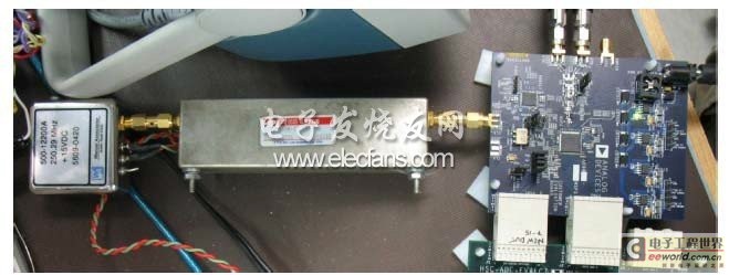
Figure 2. Sampling clock setup consisting of an oscilloscope, low-pass filter, and ADC evaluation board (from left to right).
When the analog input to the ADC is out of phase with the oscilloscope, the differential amplitude mismatch between the two signals causes a slight reduction in the fundamental power of the ADC input signal. An FFT (Fast Fourier Transform) should be used to monitor the fundamental level of the test frequency at all phase changes. Fine adjustments to the amplitude are made to ensure that the ADC is always operating at the same level. The difference in fundamental power will cause inaccurate results, indicating that the ADC is performing poorly due to inaccurate phase and fundamental power.
Figure 3 shows two FFT readings of the same device operating at the same frequency, taken using Analog Devices’ Visual Analog software. Figures 3a and 3b highlight the difference in fundamental amplitude when the phase difference between the two input signals is 0° (Figure 3a) and 20° (Figure 3b), respectively, with the second harmonic power being increased in Figure 3b.

Figure 3 a) When the phase difference between the two input signals shifts by 20° (b), the power of the second harmonic (marked as “2”) increases.
2 Testing Procedure
To begin testing, set one of the signal generators to produce a signal with a phase offset equal to 0°, and set the other signal generator so that the oscilloscope displays two waveforms that are 180° out of phase. The amplitudes of these two waveforms are close to each other, the frequencies are exactly the same, and using the oscilloscope's math functions (channel A + channel B) will result in a flat line of essentially 0 V. Note that the signal generators do not necessarily need to be set to the exact same amplitude due to errors in the generators themselves. Any differences here are caused by the reference gain and phase errors of the signal generators themselves with respect to frequency, so it is important to use the oscilloscope to zero out the phase or amplitude errors to minimize measurement errors. Next, you can have one signal generator sweep from +30° to -30° at 0° phase offset while the phase of the other signal generator remains constant.
You need to select a fundamental power and then maintain that power throughout the test. For this experiment, we set the fundamental power of each signal generator to -6 dBFS. After setting the power of the fundamental signal, the oscilloscope's math function should be used to check the phase and amplitude of the two signals. The peak-to-peak level of the math function should be as close to 0 as possible. Once the measurement system is in equilibrium, this point can be used as a 0° out-of-phase reference starting point.
Testing should include saving the ADC second and third harmonic performance for each degree of phase misalignment from +30° to -30° (relative to a reference point when the signals are 180° out of phase). As the two signals move away from 180° out of phase, the power of the carrier signal will drop as shown previously in Figure 3. Therefore, the output amplitudes of the two signal generators need to be adjusted to maintain the power level of the fundamental signal constant. An oscilloscope is used to confirm the signal amplitudes and display the signals in the time domain after any adjustments have been made. Once 30 data points have been acquired (1° offset to 30° offset), the signal generator output levels can be set so that the signals are again 180° out of phase and the amplitudes are re-adjusted to ensure that no unknown amplitude or phase drift has occurred. Repeat the above procedure for -1° to -30° offsets from the 0° reference point.
Perform measurements within the useful bandwidth of the converter or its intended application. In this experiment, we used input frequencies of 2 MHz, 70 MHz, 170 MHz, and 300 MHz, while adjusting the filter bandwidth before the splitter to support the appropriate bandwidth of the test signal.
3 Test Results
Figure 4 shows a normalized data set for input frequencies from 2 MHz to 300 MHz. Low frequencies are more tolerant to phase imbalance than high frequencies. This graph shows that the harmonic power increases with frequency. These measurements show relative measurements and are not intended to illustrate the true performance of the ADC, but rather to give you an idea of how the analog input signal changes when the phase is imbalanced.
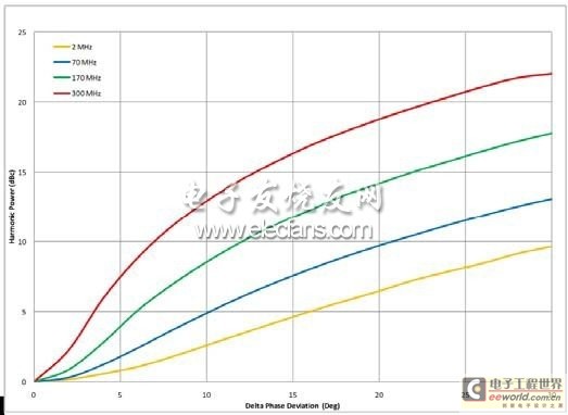
Figure 4 The second harmonic power at low frequency is lower than that at high frequency
Since positive and negative phase changes produce similar results, the harmonics generated by positive and negative offsets are averaged and normalized to zero. It can be seen from the experiment that as the frequency increases, the phase has a direct impact on the second harmonic performance of the device.
The relationship between phase deviation, simulated input frequency, and second harmonic performance is shown in a topographical plot in Figure 5. As the phase deviation increases, the input signal (dB) decreases at all frequencies, which is reflected by an increase in the second harmonic amplitude of the input signal.
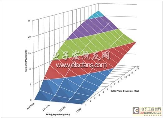
Figure 5 Relationship between second harmonic power, frequency and phase deviation
Figure 6 is similar to Figure 4, showing the third harmonic performance of the normalized input signal at each frequency. Phase deviation has much less impact on the third harmonic than on the second harmonic. The performance of the converter is flat with respect to any phase deviation at both low and high frequencies.
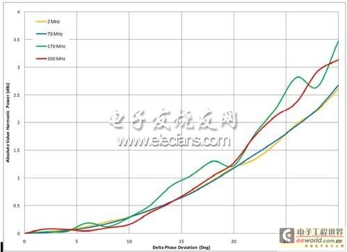
Figure 6: Regardless of the frequency, the third harmonic power is not much different
Figure 7 shows the average performance of the third harmonic in a topographical form. Just by looking at the difference in the scales, you can see that the converter’s third harmonic performance is not as closely related to frequency phase deviation as the second harmonic. This is because the odd-order nonlinearity of the ADC is primarily determined by the converter’s response to trim, calibration, design, or process limitations.
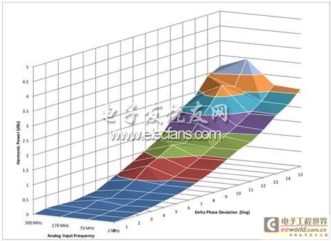
Figure 7. Relationship between harmonic power and frequency and phase shift. Explanation: The power increase is the result of phase shift, not frequency shift.
4 Conclusion
The above measurements further confirm that even-order distortion is related to balance and symmetry. It also shows that in order to achieve the data sheet performance, the front-end input network design needs to ensure that the phase deviation between the analog inputs at the ADC analog input pins (usually denoted as AIN+/- or VIN+/-) is within ±3-4°.
Previous article:Study on the Spectrum of Multi-rate Conversion Signals
Next article:Electromagnetic compatibility analysis of DCS automatic control system and frequency converter
- High signal-to-noise ratio MEMS microphone drives artificial intelligence interaction
- Advantages of using a differential-to-single-ended RF amplifier in a transmit signal chain design
- ON Semiconductor CEO Appears at Munich Electronica Show and Launches Treo Platform
- ON Semiconductor Launches Industry-Leading Analog and Mixed-Signal Platform
- Analog Devices ADAQ7767-1 μModule DAQ Solution for Rapid Development of Precision Data Acquisition Systems Now Available at Mouser
- Domestic high-precision, high-speed ADC chips are on the rise
- Microcontrollers that combine Hi-Fi, intelligence and USB multi-channel features – ushering in a new era of digital audio
- Using capacitive PGA, Naxin Micro launches high-precision multi-channel 24/16-bit Δ-Σ ADC
- Fully Differential Amplifier Provides High Voltage, Low Noise Signals for Precision Data Acquisition Signal Chain
- Innolux's intelligent steer-by-wire solution makes cars smarter and safer
- 8051 MCU - Parity Check
- How to efficiently balance the sensitivity of tactile sensing interfaces
- What should I do if the servo motor shakes? What causes the servo motor to shake quickly?
- 【Brushless Motor】Analysis of three-phase BLDC motor and sharing of two popular development boards
- Midea Industrial Technology's subsidiaries Clou Electronics and Hekang New Energy jointly appeared at the Munich Battery Energy Storage Exhibition and Solar Energy Exhibition
- Guoxin Sichen | Application of ferroelectric memory PB85RS2MC in power battery management, with a capacity of 2M
- Analysis of common faults of frequency converter
- In a head-on competition with Qualcomm, what kind of cockpit products has Intel come up with?
- Dalian Rongke's all-vanadium liquid flow battery energy storage equipment industrialization project has entered the sprint stage before production
- Allegro MicroSystems Introduces Advanced Magnetic and Inductive Position Sensing Solutions at Electronica 2024
- Car key in the left hand, liveness detection radar in the right hand, UWB is imperative for cars!
- After a decade of rapid development, domestic CIS has entered the market
- Aegis Dagger Battery + Thor EM-i Super Hybrid, Geely New Energy has thrown out two "king bombs"
- A brief discussion on functional safety - fault, error, and failure
- In the smart car 2.0 cycle, these core industry chains are facing major opportunities!
- The United States and Japan are developing new batteries. CATL faces challenges? How should China's new energy battery industry respond?
- Murata launches high-precision 6-axis inertial sensor for automobiles
- Ford patents pre-charge alarm to help save costs and respond to emergencies
- New real-time microcontroller system from Texas Instruments enables smarter processing in automotive and industrial applications
- Working principle and function of encoder
- 【LuatOS-ESP32】Series Column Preview
- HTS221 temperature and humidity sensor driver has been added to makecode
- Urgently recruiting a development engineer who knows assembly language
- Arrow Electronics Seminar: Intel FPGA Deep Learning Acceleration Technology will be held both online and offline. We look forward to your presence!
- Three safety regulations
- What are the types of triggers? What is the difference between a trigger and a latch? What are the aspects of the latch's locking and storage?
- [RISC-V MCU CH32V103 Review] ---Advancing Wiki---GPIO and TIMER
- Android desktop effect simulation based on LVGL
- We dismantled a domestic medical B-ultrasound machine and let's take a look

 Digilent Vivado library
 CLC410A8B


 京公网安备 11010802033920号