ADC Introduction:
ADC (Analog-to-Digital Converter). That is, converting analog signals into digital signals for processing. When storing or transmitting, analog-to-digital converters are almost indispensable.
The ADC peripherals integrated on the STM32 chip are very powerful. The STM32F103VET6 development board I use has an enhanced CPU. It has 18 channels and can measure 16 external and 2 internal signal sources. The A/D conversion of each channel can be performed in single, continuous, scan or intermittent mode, and the ADC result can be stored in a 16-bit data register in left-aligned or right-aligned mode.
ADC working process analysis:
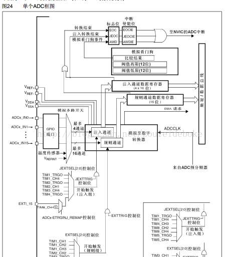
We analyze the ADC regular channel conversion process. As shown in the figure above, all devices are developed around the analog-to-digital converter in the middle. Its left end VREF+, VREF- and other ADC reference voltages, ADCx_IN0 ~ ADCx_IN15 are the ADC input signal channels, that is, some GPIO pins. The input signal is sent to the ADC device through these channels. The ADC device needs to receive a trigger signal to start the conversion, such as EXTI external trigger, timer trigger, or software trigger. After the ADC component receives the trigger signal, it samples the signal of the input channel under the drive of the ADCCLK clock and performs analog-to-digital conversion, where ADCCLK comes from the ADC prescaler.
The converted value of the ADC component is saved in a 16-bit regular channel data register (or injected channel data register). We can read it into the memory (variable) through CPU instructions or DMA. After the analog-to-digital conversion, we can trigger a DMA request or trigger an ADC conversion end event. If an analog watchdog is configured and the collected voltage is greater than the threshold, the watchdog interrupt will be triggered.
In fact, for ADC sampling, software programming is mainly about ADC configuration. Of course, I am based on DMA mode, so DMA configuration is also the key! Let's look at the code without further ado!
Main function: main.c
#include "printf.h"
#include "adc.h"
#include "stm32f10x.h"
extern __IO uint16_t ADC_ConvertedValue;
float ADC_ConvertedValueLocal;
void Delay(__IO uint32_t nCount)
{
for(;nCount !=0;nCount--);
}
int main(void)
{
printf_init();
adc_init();
printf("******This is a ADC test******\n");
while(1)
{
ADC_ConvertedValueLocal =(float) ADC_ConvertedValue/4096*3.3;
printf("The current AD value =0x%04X\n",ADC_ConvertedValue);
printf("The current AD value =%f V\n",ADC_ConvertedValueLocal);
Delay(0xffffee);
}
return 0;
}
Note that ADC_ConvertedValueLocal saves the voltage value calculated from the conversion value. The calculation formula is: actual voltage value = ADC conversion value x LSB. Here, since the reference voltage connected to VREF+ of my board is 3.3V, LSB = 3.3/4096, and the accuracy of STM32's ADC is 12 bits.
ADC and DMA configuration: adc.c
#include "adc.h"
volatile uint16_t ADC_ConvertedValue;
void adc_init()
{
GPIO_InitTypeDef GPIO_InitStructure;
ADC_InitTypeDef ADC_InitStructure;
DMA_InitTypeDef DMA_InitStructure;
RCC_AHBPeriphClockCmd(RCC_AHBPeriph_DMA1,ENABLE);
RCC_APB2PeriphClockCmd(RCC_APB2Periph_GPIOC|RCC_APB2Periph_ADC1,ENABLE);
GPIO_InitStructure.GPIO_Pin=GPIO_Pin_1;
GPIO_InitStructure.GPIO_Mode=GPIO_Mode_AIN;
GPIO_Init(GPIOC,&GPIO_InitStructure);
DMA_DeInit(DMA1_Channel1);
DMA_InitStructure.DMA_PeripheralBaseAddr = ADC1_DR_Address;//ADC地址
DMA_InitStructure.DMA_MemoryBaseAddr = (uint32_t)&ADC_ConvertedValue; //Memory address
DMA_InitStructure.DMA_DIR = DMA_DIR_PeripheralSRC; //Direction (from peripheral to memory)
DMA_InitStructure.DMA_BufferSize = 1; //Transfer content size
DMA_InitStructure.DMA_PeripheralInc = DMA_PeripheralInc_Disable; //Peripheral address fixed
DMA_InitStructure.DMA_MemoryInc = DMA_MemoryInc_Disable; //Memory address is fixed
DMA_InitStructure.DMA_PeripheralDataSize =
DMA_PeripheralDataSize_HalfWord; //Peripheral data unit
DMA_InitStructure.DMA_MemoryDataSize =
DMA_MemoryDataSize_HalfWord; //Memory data unit
DMA_InitStructure.DMA_Mode = DMA_Mode_Circular; //DMA mode: circular transmission
DMA_InitStructure.DMA_Priority = DMA_Priority_High; //Priority: High
DMA_InitStructure.DMA_M2M = DMA_M2M_Disable; //Disable memory-to-memory transfer
DMA_Init(DMA1_Channel1, &DMA_InitStructure); //Configure DMA1's 4 channels
DMA_Cmd(DMA1_Channel1,ENABLE);
ADC_InitStructure.ADC_Mode = ADC_Mode_Independent; //Independent ADC mode
ADC_InitStructure.ADC_ScanConvMode = DISABLE; //Disable scanning mode
ADC_InitStructure.ADC_ContinuousConvMode = ENABLE; // Enable continuous conversion mode
ADC_InitStructure.ADC_ExternalTrigConv = ADC_ExternalTrigConv_None; //Do not use external trigger conversion
ADC_InitStructure.ADC_DataAlign = ADC_DataAlign_Right; //Right-align the collected data
ADC_InitStructure.ADC_NbrOfChannel = 1; //Number of channels to be converted
ADC_Init(ADC1, &ADC_InitStructure);
RCC_ADCCLKConfig(RCC_PCLK2_Div8); //Configure ADC clock to be 8-divided by PCLK2, i.e. 9Hz
ADC_RegularChannelConfig(ADC1, ADC_Channel_11, 1, ADC_SampleTime_55Cycles5); //Configure ADC1 channel 11 to 55.5 sampling cycles
ADC_DMACmd(ADC1,ENABLE);
ADC_Cmd(ADC1,ENABLE);
ADC_ResetCalibration(ADC1); //Reset calibration register
while(ADC_GetResetCalibrationStatus(ADC1)); //Wait for the calibration register to be reset
ADC_StartCalibration(ADC1); //ADC calibration
while(ADC_GetCalibrationStatus(ADC1)); //Wait for calibration to complete
ADC_SoftwareStartConvCmd(ADC1, ENABLE); //Since no external trigger is used, the ADC conversion is triggered by software
}
ADC configuration is relatively simple. After all, only a single channel is configured. Let's analyze it! Here I configure the GPIO pin PC1 used by channel 11 of ADC1 to analog input mode. When used as the input of ADC, analog input must be used. For ADC channels, each ADC channel corresponds to a GPIO pin port. After the GPIO pin is set to analog input mode, it can be used to input analog voltage. STM32F103VET6 has three ADCs, and these three ADCs share 16 external channels.
The overall configuration of DMA is: using channel 1 of DMA1, data is transferred from the data register of the ADC peripheral (ADC1_DR_Address) to the memory (ADC_ConvertedValue variable), the memory peripheral address is fixed, the size of each transfer is half word (16 bits), and the DMA circular transfer mode is used.
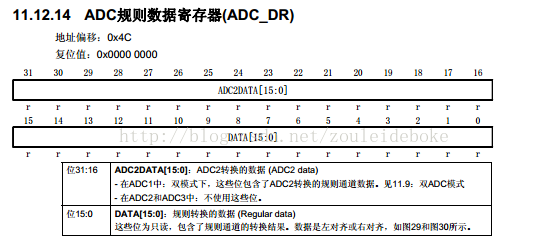
The peripheral address of DMA transfer, that is, the address of ADC1 is 0x40012400+0x4c. This address can be obtained by checking the STM32 datasheet, as shown in the figure;
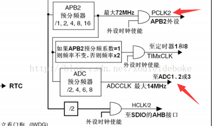
Pay special attention to the ADC conversion time configuration. Since the higher the ADC clock frequency, the faster the conversion speed, does it mean that the ADC clock frequency should be set as high as possible? In fact, this is not the case. According to the ADC clock diagram, the ADC clock has an upper limit, which cannot exceed 14MHz, as shown in the figure:
Here, the input of the ADC pre-divider is the high-speed peripheral clock (PCLK2). The RCC_ADCCLKConfig() library function is used to set the division value of the ADC pre-divider. The common clock of PCLK2 is 72MHz, and ADCCLK must be less than 14MHz, so here ADCCLK is 6 times the frequency of PCLK2, that is, 12MHz. In my program, I just set it to 8 or 9MHz. If you want the ADC to run at the highest frequency of 14MHz, you can set PCLK2 to 56MHz, and then divide it by 4 to get ACCLK.
The conversion time of ADC is not only related to the ADC clock, but also to the sampling period. Each ADC channel can be set to a different sampling period. The calculation formula for the ADC sampling time of STM32 is:
T = sampling period + 12.5 periods
The sampling period in the formula is the ADC_SampleTime configured in the function, and the 12.5 periods added later are fixed values, so the conversion time of ADC1 channel 11 is T=(55.5+12.5) x 1/9=7.56us.
Supplement: The ADC_ConvertedValue variable is defined in the adc.c file. Please note that this variable is modified by the keyword volatile. The role of volatile is to prevent the compiler from optimizing this variable. In this way, each time this variable is used, it must return to the memory of the corresponding variable to get the value. If volatile is not used for modification, the ADC_ConvertedValue variable may be directly taken from the CPU register when it is accessed (because the variable has been accessed before, that is, the value of ADC_ConvertedValue was taken from the memory and saved in a CPU register). The reason why the value is directly taken from the register instead of the memory is the result of the compiler optimizing the code (accessing the CPU register is much faster than accessing the memory). The CPU register here refers to the CPU general registers such as R0, R1, which are used for CPU calculations and temporary data storage, not the registers in the peripherals.
Because the value of the variable ADC_ConvertedValue can be changed by the DMA controller at any time, it is modified with volatile to ensure that the real-time ADC conversion value is read each time.
adc.h:
#ifndef _adc_H
#define _adc_H
#include "stm32f10x.h"
#include "stm32f10x_dma.h"
#include "stm32f10x_adc.h"
#define ADC1_DR_Address ((uint32_t)0x4001244c);
void adc_init(void);
#endif
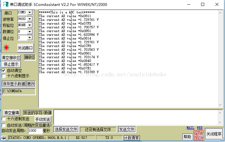
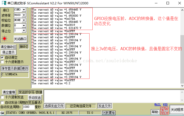
Effect picture:
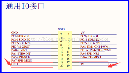
Since my development board does not have a sliding resistor, I connected the voltage input end to the 3V pin of the general IO port. As shown in the figure:
Previous article:STM32 Watchdog Summary
Next article:STM32F4 ADC1 analog watchdog [library function operation]
Recommended ReadingLatest update time:2024-11-16 17:53


 Professor at Beihang University, dedicated to promoting microcontrollers and embedded systems for over 20 years.
- Innolux's intelligent steer-by-wire solution makes cars smarter and safer
- 8051 MCU - Parity Check
- How to efficiently balance the sensitivity of tactile sensing interfaces
- What should I do if the servo motor shakes? What causes the servo motor to shake quickly?
- 【Brushless Motor】Analysis of three-phase BLDC motor and sharing of two popular development boards
- Midea Industrial Technology's subsidiaries Clou Electronics and Hekang New Energy jointly appeared at the Munich Battery Energy Storage Exhibition and Solar Energy Exhibition
- Guoxin Sichen | Application of ferroelectric memory PB85RS2MC in power battery management, with a capacity of 2M
- Analysis of common faults of frequency converter
- In a head-on competition with Qualcomm, what kind of cockpit products has Intel come up with?
- Dalian Rongke's all-vanadium liquid flow battery energy storage equipment industrialization project has entered the sprint stage before production
- Allegro MicroSystems Introduces Advanced Magnetic and Inductive Position Sensing Solutions at Electronica 2024
- Car key in the left hand, liveness detection radar in the right hand, UWB is imperative for cars!
- After a decade of rapid development, domestic CIS has entered the market
- Aegis Dagger Battery + Thor EM-i Super Hybrid, Geely New Energy has thrown out two "king bombs"
- A brief discussion on functional safety - fault, error, and failure
- In the smart car 2.0 cycle, these core industry chains are facing major opportunities!
- The United States and Japan are developing new batteries. CATL faces challenges? How should China's new energy battery industry respond?
- Murata launches high-precision 6-axis inertial sensor for automobiles
- Ford patents pre-charge alarm to help save costs and respond to emergencies
- New real-time microcontroller system from Texas Instruments enables smarter processing in automotive and industrial applications
- [RISC-V MCU CH32V103 Review] ---Advancing Wiki---GPIO and TIMER
- Android desktop effect simulation based on LVGL
- We dismantled a domestic medical B-ultrasound machine and let's take a look
- 【TI recommended course】#TI millimeter wave radar technology introduction#
- The best way to teach yourself electronics
- A brief discussion on air gap and leakage inductance
- 【GD32L233C-START Review】-3. Successful establishment of Keil development environment and DEMO routine test
- MSP432 MCU takes advantage of real-time operating systems
- M12 Gigabit Ethernet Pinout
- The Impact of IoT on Energy Efficiency



 usb_host_device_code
 【Follow me Season 2 Episode 2】Arduion UR4 homework submission code
 MCU C language programming and Proteus simulation technology (Xu Aijun)


 京公网安备 11010802033920号