Recently I needed to do some data storage, and found that the SD card was not easy to use.
Many current microcontrollers do not support SDIO, such as MSP430 (as far as I know, if there is a supported model, please let me know in time~), so I had to use SPI communication to operate the SD card. Although the follow-up involves more complicated FAT and so on, the first thing to be solved is still the problem of establishing communication.
The microcontroller model used is MSP430F5438A, and a development board is used.
SPI communication codehttp://elm-chan.org/docs/mmc/mmc_e.html
The contents are excerpted and translated for future reference.
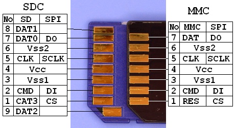
MMC card and SD card were introduced successively. Their interfaces are basically the same. The power supply is 2.7~3.6V. Do not supply 5V. Otherwise, according to the original text, it will "break down immediately" (@_@)
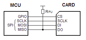
The electrical connection between the SD card and the microcontroller is shown in the figure below. 
There is a pull-up resistor, which is a bit confusing.
There are four SPI communication modes, 0 to 3, which differ in clock phase and polarity. The mode suitable for MMC and SD is mode 0 (CPHA=0, CPOL=0), but mode 3 also works in most cases.
Baidu LibraryPower ON or card insersion
After supply voltage reached 2.2 volts, wait for one millisecond at least. Set SPI clock rate between 100 kHz and 400 kHz. Set DI and CS high and apply 74 or more clock pulses to SCLK. The card will enter its native operating mode and go ready to accept native command.
Software reset
Send a CMD0 with CS low to reset the card. The card samples CS signal on a CMD0 is received successfully. If the CS signal is low, the card enters SPI mode and responds R1 with In Idle State bit (0x01). Since the CMD0 must be sent as a native command, the CRC field must have a valid value. When once the card enters SPI mode, the CRC feature is disabled and the CRC is not checked by the card, so that command transmission routine can be written with the hardcorded CRC value that valid for only CMD0 and CMD8 with the argument of zero. The CRC feature can also be switched with CMD59.
Power ON or card insersion
After supply voltage reached 2.2 volts, wait for one millisecond at least. Set SPI clock rate between 100 kHz and 400 kHz. Set DI and CS high and apply 74 or more clock pulses to SCLK. The card will enter its native operating mode and go ready to accept native command.
Software reset
Send a CMD0 with CS low to reset the card. The card samples CS signal on a CMD0 is received successfully. If the CS signal is low, the card enters SPI mode and responds R1 with In Idle State bit (0x01). Since the CMD0 must be sent as a native command, the CRC field must have a valid value. When once the card enters SPI mode, the CRC feature is disabled and the CRC is not checked by the card, so that command transmission routine can be written with the hardcorded CRC value that valid for only CMD0 and CMD8 with the argument of zero. The CRC feature can also be switched with CMD59.
Initialization
SD card in idle state, only accepts CMD0, CMD1, ACMD41, CMD58 and CMD59, and rejects any other commands. This is to read the OCR register and check the operating voltage range of the card (seems to be queried through CMD58), if the power supply is out of range, the SD card should be ejected.
The card starts the initialization process when receiving the CMD1 command. The main control chip needs to continue to send CMD1 and detect the reply to confirm that the initialization process is completed. When the R1 reply changes from 0x01 to 0x00 (Idle State bit cleared), it means that the initialization is successful. The initialization process may take hundreds of ms (the larger the card storage space, the longer the time), so a threshold for determining the timeout needs to be considered.
After the Idle State bit is cleared, general read and write commands can be executed. In addition, because ACMD41 is recommended instead of CMD1 when operating SDC, try to send ACMD41 first, and then try CMD1 after being rejected. Such a process should be able to adapt to all two cards under ideal conditions.
Initialization
In idle state, the card accepts only CMD0, CMD1, ACMD41,CMD58 and CMD59. Any other commands will be rejected. In this time, read OCR register and check working voltage range of the card. In case of the system sypply voltage is out of working voltage range, the card must be rejected. Note that all cards work at supply voltage range of 2.7 to 3.6 volts at least, so that the host contoller needs not check the OCR if supply voltage is in this range. The card initiates the initialization process when a CMD1 is received. To detect end of the initialization process, the host controller must send CMD1 and check the response until end of the initialization. When the card is initialized successfuly, In Idle State bit in the R1 response is cleared (R1 resp changes 0x01 to 0x00). The initialization process can take hundreds of milliseconds (large cards tend to longer), so that this is a consideration to determin the time out value. After the In Idle State bit cleared, generic read/write commands will able to be accepted.
Because ACMD41 instead of CMD1 is recommended for SDC, trying ACMD41 first and retry with CMD1 if rejected, is ideal to support both type of the cards.
The SCLK frequency should be set as fast as possible, which will result in better read and write performance (should be faster). The TRAN_SPEED field in the CSD register indicates the maximum clock frequency of the card. In most cases, MMC is 20MHz and SDC is 25MHz. Note that the clock frequency can be between these two values, there is no other limit with an open set in between.
On a 2GB card, the initial read and write block length may be 1024, so the block size should be reinitialized to 512 (using the CMD16 command) to work with the FAT file system.
The SCLK rate should be changed to fast as possible to maximize the read/write performance. The TRAN_SPEED field in the CSD register indicates the maximum clock rate of the card. The maximum clock rate is 20MHz for MMC, 25MHz for SDC in most case. Note that the clock rate will able to be fixed to 20/25MHz in SPI mode because there is no open-drain condition that restricts the clock rate.
The initial read/write block length can be set 1024 on 2GB cards, so that the block size should be re-initialized to 512 with CMD16 to work with FAT file system.
Initialize high-capacity cards (I don't know where the advanced part is)
After sending a CMD0 command to the card to put it into idle mode, send a CMD8 (the statement is 0x000001AA, and the correct check bit CRC is required) before initialization. If CMD8 is rejected (then a command error message 0x05 will be returned), then the card is an SDC generation 1 card or an MMC generation 3 card. If the command is accepted, an R7 reply (R1 (0x10) + 32-bit return value) will be received. The lower 12 bits of this 32-bit return value mean that the card is an SDC generation 2 card. (Then it nags about the voltage range again, which seems to be meaningless). After confirmation, start initialization: use the ACMD41 command with the HCS flag (bit30). It seems that if this bit 30 is set, the card is the well-known SDHC/SDXC card (but I am still a little unsure what the it in it is set refers to). The data read/write operations described below are based on block addressing rather than byte addressing. The data block size is fixed at 512 bytes.
Initializing high-capacity cards
After the card enters idle state with a CMD0, send a CMD8 with argument of 0x000001AA and correct CRC prior to initialization process. If the CMD8 is rejected with illigal command error (0x05), the card is SDC version 1 or MMC version 3. If accepted, R7 response (R1(0x01) + 32-bit return value) will be returned. The lower 12 bits in the return value 0x1AA means that the card is SDC version 2 and it can work at voltage range of 2.7 to 3.6 volts. If not the case, the card should be rejected. And then initiate initialization with ACMD41 with HCS flag (bit 30). After the initialization completed, read OCR register with CMD58 and check CCS flag (bit 30). When it is set, the card is a high-capacity card known as SDHC/SDXC. The data read/write operations described below are commanded in block addressing insted of byte addressing. The size of data block at block addressing mode is fixed to 512 bytes
Previous article:MSP430 SPI driver code design process
Next article:MSP430 SPI Hardware Interface
- Popular Resources
- Popular amplifiers
 Professor at Beihang University, dedicated to promoting microcontrollers and embedded systems for over 20 years.
- LED chemical incompatibility test to see which chemicals LEDs can be used with
- Application of ARM9 hardware coprocessor on WinCE embedded motherboard
- What are the key points for selecting rotor flowmeter?
- LM317 high power charger circuit
- A brief analysis of Embest's application and development of embedded medical devices
- Single-phase RC protection circuit
- stm32 PVD programmable voltage monitor
- Introduction and measurement of edge trigger and level trigger of 51 single chip microcomputer
- Improved design of Linux system software shell protection technology
- What to do if the ABB robot protection device stops
- Huawei's Strategic Department Director Gai Gang: The cumulative installed base of open source Euler operating system exceeds 10 million sets
- Download from the Internet--ARM Getting Started Notes
- Learn ARM development(22)
- Learn ARM development(21)
- Learn ARM development(20)
- Learn ARM development(19)
- Learn ARM development(14)
- Learn ARM development(15)
- Analysis of the application of several common contact parts in high-voltage connectors of new energy vehicles
- Wiring harness durability test and contact voltage drop test method
- MSP430F5529 general I/O port settings
- PWM principle PWM frequency and duty cycle detailed explanation
- TI mmWave sensors for contactless private gesture detection
- I would like to ask what specific things I need to learn to write drivers for hardware in FPGA
- Analog Discovery 2 Review (3) Frequency Response Test Tool
- Initialization and configuration of TCP/IP stack Development of network applications
- Transformer secondary side
- Help: Canaan K510 kit text display abnormal guess and solution progress
- EEWORLD University Hall----Hard Rock Technology STM32 Motor Control
- TI CC1352P dual-band multi-protocol wireless solution


 LH2111D/883B


 京公网安备 11010802033920号