I won't go into too much detail, I'll just talk about the most refined knowledge related to manufacturing.
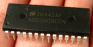
ADC0809 is a conversion IC that can convert the analog voltage signal we want to measure into a digital quantity so that it can be stored or displayed.
Below is its pin diagram and logic diagram:

Pin function description:
IN0-IN7: analog input channel. That is to say, it can measure and convert eight analog quantities in time.
ADDA-C: address line. That is to say, the different codes of these three address lines are used to select which analog quantity to measure and convert.
ALE: address latch enable signal. When the address is written to ADDA-C at a low level, the data on ADDA-C is latched when ALE jumps to a high level.
START: start conversion signal. When it is a rising edge, the internal register is cleared to 0. When it is a falling edge, the A/D conversion starts.
D0-D7: data output port. The converted digital data is output to S52 from here.
OE: output enable signal, which is the output control terminal of D0-D7. OE=0, the output terminal is in high impedance state, OE=1, and the converted data is output.
CLOCK: clock signal. There is no clock circuit inside ADC0809, and the clock pulse signal needs to be provided by the outside. Generally, it is 500KHz.
EOC: conversion end status signal. EOC=0, conversion is in progress. EOC=1, the conversion is over, and the next step of output operation can be performed
REF(+), REF(-): reference voltage. The reference voltage is used to compare with the input analog quantity as the reference for measurement. Generally, REF(=)=5v REF(-)=0V.
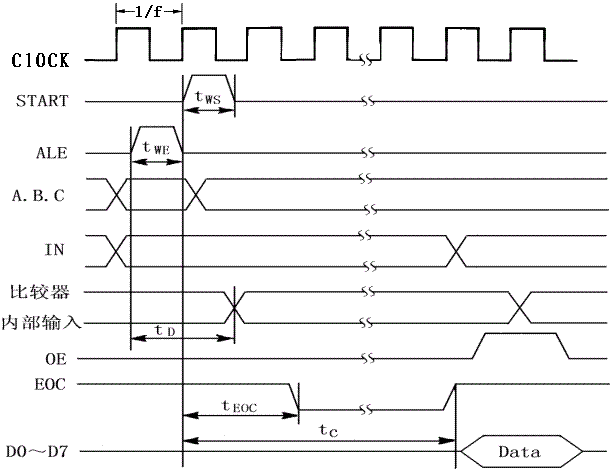
Below I will first give the timing diagram of ADC0809 and then talk about its working process: Its working process is as follows, ① 8 analog signals to be measured and converted can be connected to IN0-IN7 respectively. Someone asked, can I only connect one channel? I just want to measure one analog signal. Of course, I can carry a burden of 100 kilograms, and it is not a piece of cake for you to carry only 10 kilograms. Too much nonsense. . STOP. ② Give the ADDA-ADDC terminal the code representing the selection of the measurement channel. For example, 000(B) represents channel 0; 001(B) represents channel 1; 111 represents channel 7. ③ Set ALE from low level to high level, so as to latch the channel code sent by ADDA-ADDC, and send the analog quantity of the selected channel to the internal conversion unit after decoding. ④ Give START a positive pulse. When the rising edge occurs, all internal registers are cleared. When the falling edge occurs, the A/D conversion begins; during the conversion, START remains at a low level. ⑤ EOC is the conversion end signal. During the above A/D conversion, EOC can be continuously measured. When EOC is at a high level, it indicates that the conversion work is completed. Otherwise, it indicates that the A/D conversion is in progress. ⑥ When the A/D conversion is completed, set OE to 1, and the data of D0-D7 can be read. OE=0, the output end of D0-D7 is in a high impedance state, and OE=1, the converted data is output at the D0-D7 end. Note: The conversion work of ADC0809 is completed under the condition of clock pulse, so first give it a clock signal at the CLOCK end. The instruction manual gives the pulse signal frequency that can be connected is 10KHz-1280KHz, and the typical value is 640KHz. The teoc duration on the timing diagram is 8 clocks starting from the rising edge of START plus 2 microseconds. This should be noted, because when the START pulse just ends and enters the conversion work, EOC has not immediately become a low level, but enters a low level after 8 clock cycles, so it is best to delay the EOC detection after giving the START pulse. The conversion time of a channel is generally 64 clock cycles. For example, when the clock frequency is 640KHz, the clock cycle is 1.5625 microseconds, and the conversion time of a channel is 1.5625×64=100 microseconds, so 1000000÷100=10000 times can be converted in 1 second. Below we give a classic wiring diagram in the textbook and explain its advantages and disadvantages:

This is a drawing from an old textbook. Most of the drawings on the Internet are like this. Its clock pulse is obtained by dividing the ALE of C51 by 2. It generally means that when the crystal oscillator of C51 is 6MHz, ALE outputs a 1MHz pulse, and after dividing by 2, it gets 500KHz. But this is not applicable when we use a 12MHz crystal oscillator on S52 now. Now the pulse output by ALE of S52 is 2MHz, and after dividing by 2, it is still 1MHz.
I checked it online and found that the remedy is basically to use the T0 clock to simulate a 10KHz pulse signal. This is the minimum value allowed by the ADC0809 clock pulse. Indeed, we generally don't need such a fast conversion speed, so giving 10KHz is enough, and it also saves a divider. However, this is basically the highest frequency that can be simulated using T0.
sbit CLK=P3^3;
void main(void)
{
ET0=1;
EA=1;
TMOD=0X12;
TH0=216;
TL0=216;
TR0=1;
...
}
void t0(void) interrupt 1
{
CLK=~CLK;
}
From the above program, we can see that an interrupt occurs every 40 clock pulses. S51 is basically always busy with interrupt processing. Too frequent interrupts take up resources.
Let's take a look at the D0-D7 output port, which can only output but not write, and ADDA-ADDC can only write but not output, so we can save 74HC373. Similarly, 74LS02 can also be saved.
In this way, we save all other gate circuit ICs, including the HC373.
The purpose of simplifying the circuit is to make ADC0809 work with the least other gate circuits, so that we can focus on learning how ADC0809 works. Now let me talk about how to simulate this clock better. We are now using S52 chips. Have you ever used the T2 clock in it? It has a clock output function, as shown below:

According to the formula, with a 12MHz crystal oscillator, you can output a 45Hz-3MHz clock pulse at P1.0. It is not easy to output a 500KHz pulse.
I tried the T2 clock and it works very well:
/* This program allows the AT89S52's T2 clock to output a 45HZ square wave pulse from the P1.0 port. The P1.0 port is connected to the P3.4 port as
the external count of T0, and is output at the P2 port through the T0 clock interrupt. T0 interrupts once every 45 pulses, that is, exactly once per second*/
#include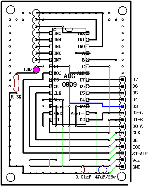 The circuit diagram is relatively simple, so I won't draw it separately. I'll just paste this circuit board diagram. D0-D7 is the data read bit, and the lower three bits D0-D2 are also connected to the A, B, and C channel selection bits. CLK is the clock pulse required by ADC0809. We will use T2 to give the clock pulse, so we must connect CLK to P1.0 of S52. In this way, OE, EOC, and ST are connected to P1.1, P1.2, and P1.3 respectively. In addition to ADC0809, there is an LED for power indication and two power filter capacitors. The following is the actual picture after it is completed:

Reference address:The use and manufacture of analog-to-digital conversion IC ADC0809... Basic knowledge


Pin function description:
IN0-IN7: analog input channel. That is to say, it can measure and convert eight analog quantities in time.
ADDA-C: address line. That is to say, the different codes of these three address lines are used to select which analog quantity to measure and convert.
ALE: address latch enable signal. When the address is written to ADDA-C at a low level, the data on ADDA-C is latched when ALE jumps to a high level.
START: start conversion signal. When it is a rising edge, the internal register is cleared to 0. When it is a falling edge, the A/D conversion starts.
D0-D7: data output port. The converted digital data is output to S52 from here.
OE: output enable signal, which is the output control terminal of D0-D7. OE=0, the output terminal is in high impedance state, OE=1, and the converted data is output.
CLOCK: clock signal. There is no clock circuit inside ADC0809, and the clock pulse signal needs to be provided by the outside. Generally, it is 500KHz.
EOC: conversion end status signal. EOC=0, conversion is in progress. EOC=1, the conversion is over, and the next step of output operation can be performed
REF(+), REF(-): reference voltage. The reference voltage is used to compare with the input analog quantity as the reference for measurement. Generally, REF(=)=5v REF(-)=0V.
Below I will first give the timing diagram of ADC0809 and then talk about its working process: Its working process is as follows, ① 8 analog signals to be measured and converted can be connected to IN0-IN7 respectively. Someone asked, can I only connect one channel? I just want to measure one analog signal. Of course, I can carry a burden of 100 kilograms, and it is not a piece of cake for you to carry only 10 kilograms. Too much nonsense. . STOP. ② Give the ADDA-ADDC terminal the code representing the selection of the measurement channel. For example, 000(B) represents channel 0; 001(B) represents channel 1; 111 represents channel 7. ③ Set ALE from low level to high level, so as to latch the channel code sent by ADDA-ADDC, and send the analog quantity of the selected channel to the internal conversion unit after decoding. ④ Give START a positive pulse. When the rising edge occurs, all internal registers are cleared. When the falling edge occurs, the A/D conversion begins; during the conversion, START remains at a low level. ⑤ EOC is the conversion end signal. During the above A/D conversion, EOC can be continuously measured. When EOC is at a high level, it indicates that the conversion work is completed. Otherwise, it indicates that the A/D conversion is in progress. ⑥ When the A/D conversion is completed, set OE to 1, and the data of D0-D7 can be read. OE=0, the output end of D0-D7 is in a high impedance state, and OE=1, the converted data is output at the D0-D7 end. Note: The conversion work of ADC0809 is completed under the condition of clock pulse, so first give it a clock signal at the CLOCK end. The instruction manual gives the pulse signal frequency that can be connected is 10KHz-1280KHz, and the typical value is 640KHz. The teoc duration on the timing diagram is 8 clocks starting from the rising edge of START plus 2 microseconds. This should be noted, because when the START pulse just ends and enters the conversion work, EOC has not immediately become a low level, but enters a low level after 8 clock cycles, so it is best to delay the EOC detection after giving the START pulse. The conversion time of a channel is generally 64 clock cycles. For example, when the clock frequency is 640KHz, the clock cycle is 1.5625 microseconds, and the conversion time of a channel is 1.5625×64=100 microseconds, so 1000000÷100=10000 times can be converted in 1 second. Below we give a classic wiring diagram in the textbook and explain its advantages and disadvantages:


I checked it online and found that the remedy is basically to use the T0 clock to simulate a 10KHz pulse signal. This is the minimum value allowed by the ADC0809 clock pulse. Indeed, we generally don't need such a fast conversion speed, so giving 10KHz is enough, and it also saves a divider. However, this is basically the highest frequency that can be simulated using T0.
sbit CLK=P3^3;
void main(void)
{
ET0=1;
EA=1;
TMOD=0X12;
TH0=216;
TL0=216;
TR0=1;
...
}
void t0(void) interrupt 1
{
CLK=~CLK;
}
From the above program, we can see that an interrupt occurs every 40 clock pulses. S51 is basically always busy with interrupt processing. Too frequent interrupts take up resources.
Let's take a look at the D0-D7 output port, which can only output but not write, and ADDA-ADDC can only write but not output, so we can save 74HC373. Similarly, 74LS02 can also be saved.
In this way, we save all other gate circuit ICs, including the HC373.
The purpose of simplifying the circuit is to make ADC0809 work with the least other gate circuits, so that we can focus on learning how ADC0809 works. Now let me talk about how to simulate this clock better. We are now using S52 chips. Have you ever used the T2 clock in it? It has a clock output function, as shown below:

I tried the T2 clock and it works very well:
/* This program allows the AT89S52's T2 clock to output a 45HZ square wave pulse from the P1.0 port. The P1.0 port is connected to the P3.4 port as
the external count of T0, and is output at the P2 port through the T0 clock interrupt. T0 interrupts once every 45 pulses, that is, exactly once per second*/
#include
 The circuit diagram is relatively simple, so I won't draw it separately. I'll just paste this circuit board diagram. D0-D7 is the data read bit, and the lower three bits D0-D2 are also connected to the A, B, and C channel selection bits. CLK is the clock pulse required by ADC0809. We will use T2 to give the clock pulse, so we must connect CLK to P1.0 of S52. In this way, OE, EOC, and ST are connected to P1.1, P1.2, and P1.3 respectively. In addition to ADC0809, there is an LED for power indication and two power filter capacitors. The following is the actual picture after it is completed:
Previous article:MAX7219 driver (LED display chip)
Next article:Keil or c51 assembly calls C language functions easily overlooked issues
- Popular Resources
- Popular amplifiers
Recommended Content
Latest Microcontroller Articles
He Limin Column
Microcontroller and Embedded Systems Bible
 Professor at Beihang University, dedicated to promoting microcontrollers and embedded systems for over 20 years.
MoreSelected Circuit Diagrams
MorePopular Articles
- LED chemical incompatibility test to see which chemicals LEDs can be used with
- Application of ARM9 hardware coprocessor on WinCE embedded motherboard
- What are the key points for selecting rotor flowmeter?
- LM317 high power charger circuit
- A brief analysis of Embest's application and development of embedded medical devices
- Single-phase RC protection circuit
- stm32 PVD programmable voltage monitor
- Introduction and measurement of edge trigger and level trigger of 51 single chip microcomputer
- Improved design of Linux system software shell protection technology
- What to do if the ABB robot protection device stops
MoreDaily News
- Keysight Technologies Helps Samsung Electronics Successfully Validate FiRa® 2.0 Safe Distance Measurement Test Case
- Innovation is not limited to Meizhi, Welling will appear at the 2024 China Home Appliance Technology Conference
- Innovation is not limited to Meizhi, Welling will appear at the 2024 China Home Appliance Technology Conference
- Huawei's Strategic Department Director Gai Gang: The cumulative installed base of open source Euler operating system exceeds 10 million sets
- Download from the Internet--ARM Getting Started Notes
- Learn ARM development(22)
- Learn ARM development(21)
- Learn ARM development(20)
- Learn ARM development(19)
- Learn ARM development(14)
Guess you like
- Guys, please help me find out what the problem is.
- I would like to ask about the interrupt problem of msp430f5529
- Three questions on embedded ARM basics
- [Rawpixel RVB2601 development board trial experience] GRB breathing light
- Dancing flame pendant
- Do you purchase samples or apply for them for free?
- SDK BLE example project command line compilation (HeartRate device)
- EEWorld interviews Toshiba PCIM booth engineer: 2-minute short video shows you key products and solutions
- Is it necessary to learn TI's KeystoneII series multi-core heterogeneous processors?
- cc2540 cc2541 low power consumption measurement and summary - and precautions - low power consumption less than 10uA

 OPA353UA/2K5


 京公网安备 11010802033920号