Now everyone uses S52, why use C2051! The price is similar. But the size of C2051 is much smaller than S51 and S52, and it has only 20 pins. In some simple controls, these pins are enough, and the small size is more advantageous. But it seems that there is no S2051 that supports online programming (ISP) at present. So I tried to make a C2051 programmer, and more importantly, I want to share with you the hardware and software debugging skills in the process of circuit manufacturing, and try to achieve the experience and methods of success at one time. I
searched the Internet and found many pictures, which are similar. The most common picture above: The above picture is a circuit that can burn many devices, and its PCB board is also easy to find on the Internet. But because it is an experimental production, there is no PCB, so I will use a universal board. Since wide-body devices all support ISP, I removed the 40-pin wide-body IC socket and only left a 20-pin narrow-body IC socket for burning C2051. After modifying the circuit, the circuit diagram is as follows:
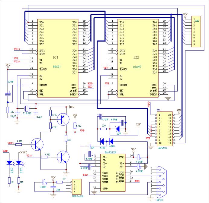

The component list is as follows:
1/8w 4.7k 6 (6 in total)
560r 3 (3 in total)
2k2 1
4.7 ohm 1 connected in series with the power supply circuit for protection
10k resistor 1 used for CPU p0 port pull-up
1n4148 2 used for vpp high voltage supply (note that one end of 4148 is black)
12v 1 used for vpp high voltage supply (note that one end of 12V is white, don't get confused)
4.7uf/50v 8 Use the same model for all electrolytics, pay attention to the direction
104 2 used for power supply filtering
22p 2 used for crystal circuit
11.0592 1 crystal
2n5401 1 Pay attention to the model and the direction of insertion, don't make a mistake!
2n5551 2
LEDs 2 3mm white and red (for power indication and communication indication) (pay attention to the direction)
db9 1 serial port
20pin card holder 1 burn 2051 etc.
40pin ic holder 1 insert monitoring 89s51
16pin ic holder 1 insert max232 chip
usb holder 1 serial
port cable for power supply 1 usb cable for communication 1 At89s51 for
power supply 1 for monitoring max232cpe 1 integrated circuit pcb for communication 1 The actual circuit board has been made today, let's show it first. Then I will talk about the detailed debugging methods and steps:

(Click to see the full picture)
This circuit may be a little complicated for beginners. It is divided into several parts. If you plan the circuit board first, then solder all the components at once, and then debug, the probability of success is very small. So what should you do? First plan the position layout of the components, then divide it into several units, debug after a unit is completed, and then proceed to the production and debugging of the next unit after it is normal. My plan is as follows, first the power supply part including the power indicator LED:

First, solder the USB socket, and then plug in the USB power supply after confirming that there is no short circuit. Use a multimeter to find out which of the two points A and B is the positive pole of 5v and which is the ground. Then remove the power supply and solder the remaining capacitors, resistors and LEDs. After confirming that there is no short circuit, connect the power supply and the LED should light up. I changed the current limiting resistor of the LED to 2K because I think it is bright enough. The current is 1.5 mA. The actual object is as shown in the red circle on the right. The
second part is MAX232, including the +12v voltage regulator circuit. MAX232 is a special IC for TTL to RS232. It provides a positive 10v and negative 10v boost circuit inside. We used its boost circuit to obtain a +12v power supply.
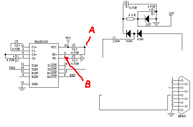
We first solder the 9-pin serial port, but do not connect the MAX232. In the MAX232 area you planned, solder the MAX232 socket and four capacitors according to the circuit on the left side of the above figure. After checking that there is no short circuit, plug in the MAX232 and connect the power supply. The voltage of +9v-+10v should be measured at point A. There should be a voltage of -9v--10v at point B. Connect pin 10 to the ground, and pin 7 should be +10V. If pin 10 is connected to +5v, then pin 7 becomes -10v. In this way, the MAX232 is normal. Connect pin 2 of the serial port to pin 7 of the MAX232. Connect pin 3 of the serial port to pin 8 of the MAX232. Connect the power and connect pin 10 of the MAX232 to ground and +5v respectively to see if pin 2 of the serial port changes as before. After the above debugging is correct, solder the 12V voltage regulator circuit on the right side of the above figure. As shown below:
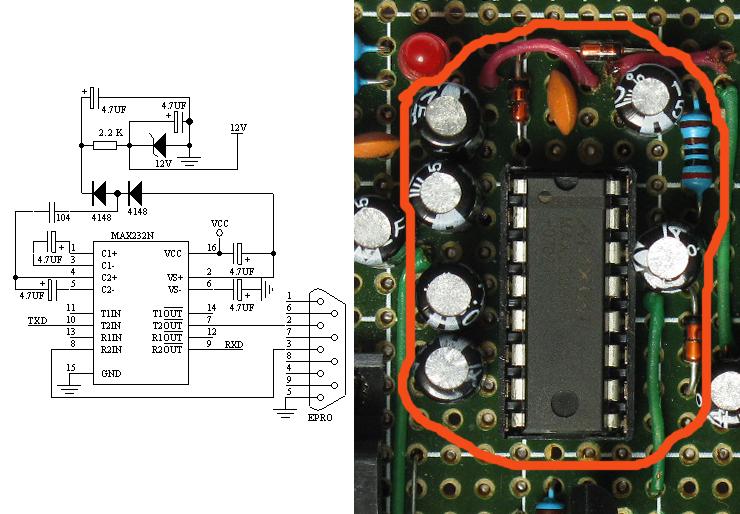
Use a multimeter to measure a stable +12V voltage at both ends of the voltage regulator. In this way, your serial port conversion and 12v power supply circuit are debugged normally.
The third part is the 12V burning control part: the circuit and the actual picture are as follows:

After this part of the circuit is soldered, connect the normal +12v and power supply +5V of the second part. First measure whether the +12v access point and the power supply voltage +5v on the circuit are normal. Then measure point A in the above figure, which should also be +5v. Then you connect VO13 to +5V with a wire, so point A is +9v-+11v. Good! Disconnect VO13, and then connect V014 to +5v with a wire, and point A should be close to 0. In this way, the 12V burning control circuit is also debugged correctly.
The following is the circuit of the S51 part, as shown below:

This part of the circuit includes the pull-up resistor of the P0 port and the receiving indicator LED connected to the 10th pin of S51. Don't forget to connect the 31st pin (EA/VP) of S51 to the power supply +5v. First make sure that the connection between the 9th pin of MAX232 and the 10th pin of S51 is disconnected (because the 9th pin of MAX232 will output +5v high level after debugging normally, which will light up the receiving indicator LED and hinder the inspection of the working performance of S51). After checking that the circuit is correct, plug in the S51 chip and connect the power supply. The static current should be around 9-12mA. Good! Open KEIL and write a test program:
#include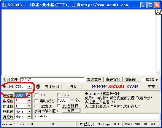 Set the baud rate of the red circle to 19200. Confirm it is COM1 port. Then power on the 2051 programmer, and "hello world" will appear on my PC serial debugger immediately.

In this way, the serial communication with the PC is debugged successfully. If you do not get the correct result, and the debugging in the above steps is normal, then there is an error in the wiring from the PC serial port to your S51. Check your wiring carefully and you will find the error.
After the above steps are normal, it is time to integrate the circuits that have been debugged normally in these steps. Connect the 12v burning control terminal VPP to the 1st pin of 2051, and connect VO13 and VO14 to the 13th and 14th pins of S51 respectively. Connect the 15th pin VST of S51 to the 9th pin of 2051. Connect the 1st pin (P1.0) of S51 to the 11th pin of 2051. Connect the 5th, 6th, 7th and 8th pins of S51 to the 5th, 6th, 7th and 8th pins of 2051 respectively. Connect the P0 port (pins 32-39) of S51 to the 12th-19th pins of 2051 respectively. Don't forget to connect the power supply and ground of 2051.

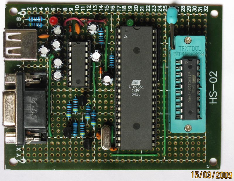
OK! After checking everything, connect the power supply and try again to see if the serial communication is normal (to prevent the S51 from not working due to incorrect soldering after soldering). Unplug the S51, use ISP to write the E51Pro.HEX driver firmware into the S51, and then plug it into the 40-pin S51 socket, plug the AT89C2051 into the 20-pin IC socket, connect the PC serial port, run the Easy 51Pro V2.0 on the PC, and then power on the 2051 burner. Select AT89C2051 on the PC software, click on the device detection, mine is 1e 21 FF. Then try to open a HEX file, click on auto-complete, it will complete the device detection, erasing, writing, verification and other tasks, as shown below:
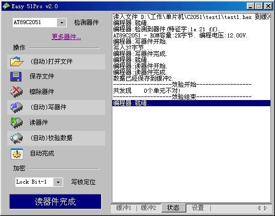
If your device is not found, but the previous serial communication and other debugging are normal, then the wiring in your last step may be wrong. Carefully check your wiring, and whether the power supply and grounding of the C2051 socket are normal.
OK, dust it off, it's done. Finally, I can go to the side to drink some tea and cool down for a while! Give some applause! Is it easy? I... !
Summary: Developing the habit of debugging step by step is very beneficial to the success of the circuit. If there is a problem, the scope of debugging can be minimized.
Keywords:AT89C2051
Reference address:Manufacturing and debugging of AT89C2051 programmer
searched the Internet and found many pictures, which are similar. The most common picture above: The above picture is a circuit that can burn many devices, and its PCB board is also easy to find on the Internet. But because it is an experimental production, there is no PCB, so I will use a universal board. Since wide-body devices all support ISP, I removed the 40-pin wide-body IC socket and only left a 20-pin narrow-body IC socket for burning C2051. After modifying the circuit, the circuit diagram is as follows:


1/8w 4.7k 6 (6 in total)
560r 3 (3 in total)
2k2 1
4.7 ohm 1 connected in series with the power supply circuit for protection
10k resistor 1 used for CPU p0 port pull-up
1n4148 2 used for vpp high voltage supply (note that one end of 4148 is black)
12v 1 used for vpp high voltage supply (note that one end of 12V is white, don't get confused)
4.7uf/50v 8 Use the same model for all electrolytics, pay attention to the direction
104 2 used for power supply filtering
22p 2 used for crystal circuit
11.0592 1 crystal
2n5401 1 Pay attention to the model and the direction of insertion, don't make a mistake!
2n5551 2
LEDs 2 3mm white and red (for power indication and communication indication) (pay attention to the direction)
db9 1 serial port
20pin card holder 1 burn 2051 etc.
40pin ic holder 1 insert monitoring 89s51
16pin ic holder 1 insert max232 chip
usb holder 1 serial
port cable for power supply 1 usb cable for communication 1 At89s51 for
power supply 1 for monitoring max232cpe 1 integrated circuit pcb for communication 1 The actual circuit board has been made today, let's show it first. Then I will talk about the detailed debugging methods and steps:

(Click to see the full picture)

second part is MAX232, including the +12v voltage regulator circuit. MAX232 is a special IC for TTL to RS232. It provides a positive 10v and negative 10v boost circuit inside. We used its boost circuit to obtain a +12v power supply.


The third part is the 12V burning control part: the circuit and the actual picture are as follows:

The following is the circuit of the S51 part, as shown below:

This part of the circuit includes the pull-up resistor of the P0 port and the receiving indicator LED connected to the 10th pin of S51. Don't forget to connect the 31st pin (EA/VP) of S51 to the power supply +5v. First make sure that the connection between the 9th pin of MAX232 and the 10th pin of S51 is disconnected (because the 9th pin of MAX232 will output +5v high level after debugging normally, which will light up the receiving indicator LED and hinder the inspection of the working performance of S51). After checking that the circuit is correct, plug in the S51 chip and connect the power supply. The static current should be around 9-12mA. Good! Open KEIL and write a test program:
#include
 Set the baud rate of the red circle to 19200. Confirm it is COM1 port. Then power on the 2051 programmer, and "hello world" will appear on my PC serial debugger immediately.
After the above steps are normal, it is time to integrate the circuits that have been debugged normally in these steps. Connect the 12v burning control terminal VPP to the 1st pin of 2051, and connect VO13 and VO14 to the 13th and 14th pins of S51 respectively. Connect the 15th pin VST of S51 to the 9th pin of 2051. Connect the 1st pin (P1.0) of S51 to the 11th pin of 2051. Connect the 5th, 6th, 7th and 8th pins of S51 to the 5th, 6th, 7th and 8th pins of 2051 respectively. Connect the P0 port (pins 32-39) of S51 to the 12th-19th pins of 2051 respectively. Don't forget to connect the power supply and ground of 2051.


OK, dust it off, it's done. Finally, I can go to the side to drink some tea and cool down for a while! Give some applause! Is it easy? I... !
Summary: Developing the habit of debugging step by step is very beneficial to the success of the circuit. If there is a problem, the scope of debugging can be minimized.
Previous article:74LS165 C51 program (incorporated into outgoing chip)
Next article:Clock program (LED+DS1302+AT89S52)
- Popular Resources
- Popular amplifiers
Recommended Content
Latest Microcontroller Articles
- Learn ARM development(16)
- Learn ARM development(17)
- Learn ARM development(18)
- Embedded system debugging simulation tool
- A small question that has been bothering me recently has finally been solved~~
- Learn ARM development (1)
- Learn ARM development (2)
- Learn ARM development (4)
- Learn ARM development (6)
He Limin Column
Microcontroller and Embedded Systems Bible
 Professor at Beihang University, dedicated to promoting microcontrollers and embedded systems for over 20 years.
MoreSelected Circuit Diagrams
MorePopular Articles
- LED chemical incompatibility test to see which chemicals LEDs can be used with
- Application of ARM9 hardware coprocessor on WinCE embedded motherboard
- What are the key points for selecting rotor flowmeter?
- LM317 high power charger circuit
- A brief analysis of Embest's application and development of embedded medical devices
- Single-phase RC protection circuit
- stm32 PVD programmable voltage monitor
- Introduction and measurement of edge trigger and level trigger of 51 single chip microcomputer
- Improved design of Linux system software shell protection technology
- What to do if the ABB robot protection device stops
MoreDaily News
- Analysis of the application of several common contact parts in high-voltage connectors of new energy vehicles
- Wiring harness durability test and contact voltage drop test method
- From probes to power supplies, Tektronix is leading the way in comprehensive innovation in power electronics testing
- From probes to power supplies, Tektronix is leading the way in comprehensive innovation in power electronics testing
- Sn-doped CuO nanostructure-based ethanol gas sensor for real-time drunk driving detection in vehicles
- Design considerations for automotive battery wiring harness
- Do you know all the various motors commonly used in automotive electronics?
- What are the functions of the Internet of Vehicles? What are the uses and benefits of the Internet of Vehicles?
- Power Inverter - A critical safety system for electric vehicles
- Analysis of the information security mechanism of AUTOSAR, the automotive embedded software framework
Guess you like
- First Battlefield
- Infrared remote control LED dot matrix
- [Chuanglong TL570x-EVM] Install Prossessor SDK and create a development environment
- NRK3301 speech recognition chip schematic
- Microchip Live Today: How to Build a Car Charger
- Share some of my experiences as a part-time communication designer
- EEWORLD University Hall----Live Replay: Energy Saving and Carbon Reduction-Omron Relay, Switch, and Connector Solutions for Photovoltaic Inverter/Energy Storage Systems
- Nonlinear Compensation Method for Sensor Bridge Circuit
- DIY_boostxl-k350qvg under the recent proofing storm
- Today is 520, another beautiful day for confession. What actions will you take?

 ADA10001S3C


 京公网安备 11010802033920号