Principle:
I2C bus is a two-wire bus used to connect IC devices. It transmits information between devices connected to the bus through two lines, SDA (serial data line) and SCL (serial clock line), and identifies each device according to the address: whether it is a single-chip microcomputer, memory, LCD driver or keyboard interface. The
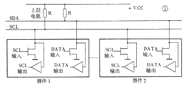
I2C bus interface circuit structure is shown in the figure.

Both SDA and SCL are bidirectional I/O lines, connected to the positive power supply through a pull-up resistor. When the bus is idle, both lines are high. The output stage of the device connected to the bus must be open collector or drain to have a line "AND" function. The data transfer rate of the I2C bus is 100kbit/s in the standard working mode, and the maximum transfer rate can reach 400kbit/s in the fast mode.
In the I2C bus technical specification, the definition of the start and end signals (also called start and stop signals) is shown in the figure. When the clock line SCL is high, the data line SDA jumps from high level to low level, which is defined as the "start" signal; when the SCL line is high, the SDA line jumps from low level to high level, which is the "end" signal. Both the start and end signals are generated by the master device. After the start signal, the bus is considered to be busy; for a period of time after the end signal, the bus is considered to be idle.

The data transmission format of the I2C bus is: after the I2C bus start signal, the first byte of data sent out is used to select the slave device address, of which 4-7 bits are the device code, such as 1010 represents a serial E2PROM device. 1-3 bits are the chip select address of the memory or the block address code in the memory. How to distinguish? I will explain it in detail later. The 8th bit is the direction bit (R/W). The direction bit is "0" to indicate sending, that is, the master device writes information to the selected slave device; the direction bit is "1" to indicate that the master device will read information from the slave device. After the start signal, each device in the system compares its own address with the address sent by the master device to the bus. If it is consistent with the address sent by the master device to the bus, then the device is the device addressed by the master device, and whether it receives or sends information is determined by the 8th bit (R/W).
The process of a byte write operation: First, after the device sends a start signal, the sending device identifies the control byte, that is, 1010A2A1A00 (the lowest position is 0, that is, the R/W read and write control bit is low level 0), and then waits for the response signal to indicate that the slave device is addressed. Then send an AT24CXX memory location address to be written. After waiting for the AT24CXX response signal again, the data byte will be sent, and the AT24CXX will write it to the memory address just specified after receiving it. Then the master device waits for the AT24CXX response signal again. The master device finally sends a stop signal.
The number of data bytes transmitted each time on the I2C bus is unlimited, but each byte must be 8 bits, and each transmitted byte must be followed by an acknowledgment bit (9th bit), also called an acknowledgement bit (ACK). The data transmission process is shown in the figure. Each time, the highest bit is transmitted first. Usually, the slave device will respond after receiving each byte, that is, release the SCL line to return to a high level, ready to receive the next data byte, and the master device can continue to transmit. If the slave device is processing a real-time event and cannot receive data (for example, it is processing an internal interrupt and cannot receive data bytes on the I2C bus before the interrupt is processed), the clock SCL line can be kept at a low level, and the slave device must keep SDA at a high level. At this time, the master device generates an end signal, causing the transmission to end abnormally, forcing the master device to wait. When the slave device completes the processing, it will release the SCL line and the master device will continue to transmit.

After the master device sends a byte of data, it then sends a clock (ACK) recognition bit corresponding to the SCL line. During this clock, the master device releases the SDA line, and the transmission of a byte is completed. The response signal of the slave device pulls the SDA line to a low level, making SDA a stable low level during the high level of the clock. After the response signal of the slave device ends, the SDA line returns to a high level and enters the next transmission cycle.
The I2C bus also has the function of using a general call address to address all devices on the bus. If a device does not need any data provided in the general call addressing, it can ignore the address and not respond. If the device needs the data provided in the general call addressing, it should respond to the address, which behaves as a receiver.
5. There may be multiple devices connected to the arbitration bus for bus contention, and sometimes two or more master devices may want to occupy the bus at the same time. For example, in a multi-microcontroller system, there may be two microcontrollers that want to send data to the bus at the same time at a certain moment. This situation is called bus contention. The I2C bus has multi-master capability and can arbitrate bus contention on the SDA line. The arbitration principle is as follows: when multiple master devices want to occupy the bus at the same time, if a master device sends a high level and another master device sends a low level, the device whose sending level does not match the SDA bus level at this time will automatically shut down its output stage. The arbitration of bus contention is carried out at two levels. The first is the comparison of address bits. If the master device addresses the same slave device, the comparison of data bits is entered, thereby ensuring the reliability of contention arbitration. Since arbitration is carried out using information on the I2C bus, no information loss will occur.
Device Description:
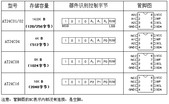
The AT24CXXX series pin diagram is as follows

Now let me talk about the specific use of AT24CXX.
Assume that P0.0 of AT89S51 is used as SDA bus and P0.1 is used as SCL bus. There are several I2C devices connected to SDA and SCL buses.
Now we need to write byte to E2PROM_01 memory to see how it is found.
As mentioned above, after sending a start signal, a byte of device identification signal is sent. Bits 4 to 7 of this byte are the device identification code. 1010 corresponds to E2PROM device, and other devices are ignored. Bits 1 to 3 are the physical address of the device, that is, if it is E2PROM, it can connect (000-111) 8 E2PROMs on the I2C bus. Here we have to talk in detail about the relationship between A0, A1, A2 on AT24CXX and this device identification byte. As mentioned above, the addressing range of the memory is one byte, which is 256. The storage capacity of AT24C02 is 256 words, which just uses up one byte of address. The three pins A0, A1, and A2 on the device circuit match the device identification control byte sent by AT89S51 by connecting high or low levels, so as to identify the memory that AT89S51 will operate. Now the capacity of AT24C04 is 512 bytes, so isn't one byte address enough? In fact, it divides 512 bytes into two pages, 256 bytes per page, and the page address is 1 bit of the device identification control byte. As mentioned earlier, aren't these 1-3 bits matched with A0, A1, and A2 on the device to identify the device? Yes, but the situation changes when the memory capacity exceeds 256 bytes. A0 on AT24C04 is now abandoned, and only A1 and A2 are used. In this way, only four AT24C04s (00-11) can be connected. Similarly, AT24C08 has a capacity of 1K bytes and is divided into 4 pages. Therefore, the page address is the 1-2 bits of the device identification control byte. A0 and A1 on the device are abandoned, and only A2 is used. Only two AT24C08s can be connected. AT24C16 has a capacity of 2K bytes and is divided into 8 pages. The page address is the 1-3 bits of the device identification control byte, all of which are used. A0, A1, and A2 on the device are invalid, and only one AT24C16 can be connected.

Do you understand what I mean?
For the large-capacity AT24C32-1024 memory, the device's storage address is two bytes, so its one page is 65536 (64K). The capacity of AT24C32-64 is 4K bytes to 8K bytes, and 8 devices can be connected in one page. The device code of AT24C128-1024 was also changed from 1010 to 10100, with one more bit, and the device physical address that identifies the control byte has one less bit, becoming 1-2 bits, and the corresponding A2 on the device pin is also abandoned and vacant, so only four devices can be connected at most. AT24C128-512 has only two device addresses, so only four devices can be connected at most. The capacity of AT24C1024 is 128K, divided into two pages, and the 1 bit of the control byte is used as the page address. The A0 pin of the device is abandoned and only A1 is used. Therefore, only 2 devices can be connected.

Next, we will proceed with the specific production. First, prepare the device as shown below. I use AT24C16

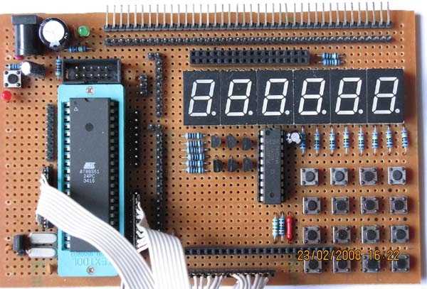
The original board is as follows

After welding.

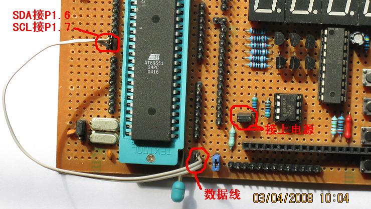
OK! Now let's debug: plug in the main power supply. But do not connect the short-circuit cap of the AT24C16 power supply. Connect the current range of the multimeter between the two pins of the short-circuit cap to check whether there is a short circuit and the size of the static current. The measured static current is almost zero. When the level of the two data lines is changed, the current will increase, indicating that the circuit is basically normal.

Now we connect the power short-circuit cap and the AT24C16 power supply. Use jumpers to connect the two data lines to the P1.6 and P1.7 ports (you can choose which port to connect to). Pay attention to distinguish which is SDA and which is SCL. Don't make a mistake.

After installing LCD12864, we will debug the software.

In the next article, we will debug the software part.
Previous article:The basic principle and usage of 12864 dot matrix LCD
Next article:AT89S51 Minimum System Production
Recommended ReadingLatest update time:2024-11-16 15:40
- Popular Resources
- Popular amplifiers
-
 Teach you to learn 51 single chip microcomputer-C language version (Second Edition) (Song Xuefeng)
 -
 EDA Technology Practical Tutorial--Verilog HDL Edition (Sixth Edition) (Pan Song, Huang Jiye)
 -
 Learn C language for AVR microcontrollers easily (with video tutorial) (Yan Yu, Li Jia, Qin Wenhai)
 -
 Learn to repair variable frequency air conditioner easily with zero basic knowledge (Zhang Yunkun and Zhang Xinde)
 Professor at Beihang University, dedicated to promoting microcontrollers and embedded systems for over 20 years.
- Innolux's intelligent steer-by-wire solution makes cars smarter and safer
- 8051 MCU - Parity Check
- How to efficiently balance the sensitivity of tactile sensing interfaces
- What should I do if the servo motor shakes? What causes the servo motor to shake quickly?
- 【Brushless Motor】Analysis of three-phase BLDC motor and sharing of two popular development boards
- Midea Industrial Technology's subsidiaries Clou Electronics and Hekang New Energy jointly appeared at the Munich Battery Energy Storage Exhibition and Solar Energy Exhibition
- Guoxin Sichen | Application of ferroelectric memory PB85RS2MC in power battery management, with a capacity of 2M
- Analysis of common faults of frequency converter
- In a head-on competition with Qualcomm, what kind of cockpit products has Intel come up with?
- Dalian Rongke's all-vanadium liquid flow battery energy storage equipment industrialization project has entered the sprint stage before production
- Allegro MicroSystems Introduces Advanced Magnetic and Inductive Position Sensing Solutions at Electronica 2024
- Car key in the left hand, liveness detection radar in the right hand, UWB is imperative for cars!
- After a decade of rapid development, domestic CIS has entered the market
- Aegis Dagger Battery + Thor EM-i Super Hybrid, Geely New Energy has thrown out two "king bombs"
- A brief discussion on functional safety - fault, error, and failure
- In the smart car 2.0 cycle, these core industry chains are facing major opportunities!
- The United States and Japan are developing new batteries. CATL faces challenges? How should China's new energy battery industry respond?
- Murata launches high-precision 6-axis inertial sensor for automobiles
- Ford patents pre-charge alarm to help save costs and respond to emergencies
- New real-time microcontroller system from Texas Instruments enables smarter processing in automotive and industrial applications
- There is no one to teach me how to learn FPGA. Can I learn it just by watching tutorials?
- Brushed DC and brushless DC driver chips
- Analysis of the application of NTC thermistor in power circuit
- Use LabVIEW to remotely control the Raspberry Pi via WiFi~
- Analysis of the working principles of seven triode collector DC circuits 6
- What is PENA in the technical manual spnu515c.pdf of TMS570LS1227? ? ?
- This switching circuit
- Analog Discovery 2 Review (7) Exploring the Implementation of an Impedance Analyzer
- EFINIX FPGA Video Image Learning Solution - Open Source
- Combination of TM1640 and PIC12F629 microcontroller

 Teach you to learn 51 single chip microcomputer-C language version (Second Edition) (Song Xuefeng)


 京公网安备 11010802033920号