XC866 is the first generation of the new 8-bit microcontroller series (XC800), integrating a high-performance 8051 core, on-chip FLASH and a powerful peripheral set. In addition, the XC800 series products have an on-chip oscillator and an embedded voltage regulator (EVR) that supports 3.3V or 5.0V single power supply, which further enhances product performance and effectively saves system costs. In addition to products with on-chip FLASH, XC866 also launches ROM-compatible products in the same series, providing further cost savings for mass production.
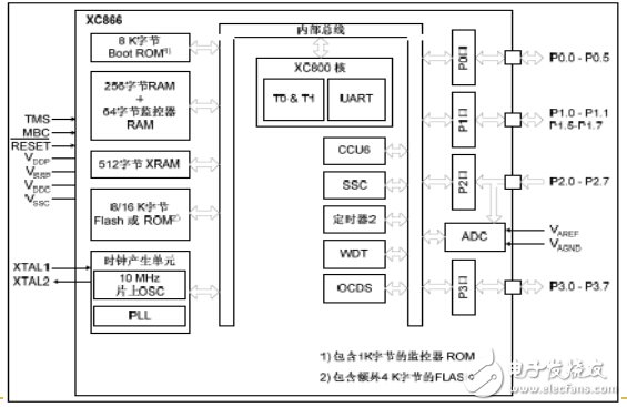
MCU structure diagram
Pin Diagram
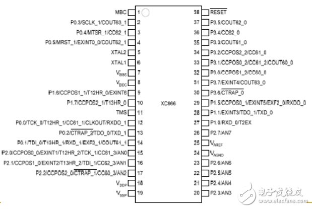
Multi-function pin examples
-P0.0 pin 12
TCK_0 JTAG clock input
T12HR_1 CCU6 Timer 12 Hardware Run Input
CC61_1 Capture/Compare Channel 1 Input/Output
CLKOUT Clock output
RXDO_1 UART transmit data output
-P0.1 Pin 14
TDI_0 JTAG serial data input
T13HR_1 CCU6 Timer 13 Hardware Run Input
RXD_1 UART receive data input
COUT61_1 Capture/Compare Channel 1 Output
EXF2_1 Timer 2 external flag output
Module Analysis
Memory structure
-8K boot ROM address: C00H-E000H
-256 bytes of on-chip RAM, 0~7FH use direct addressing, 80~FFH use
(1) Register indirect addressing
-128 bytes SFR address 80~FFH, using direct addressing
-512 bytes XRAM address F000~F200, accessed using MOVX. When using R0 and R1 as address registers, the high-order address of the XRAM address is defined by the value in register XADDRH.
-8K/16K program memory, starting address 0000
- Special EO register operation, allowing toggle DPTR and program ROM
- Write operation (instruction: MOVC @ (DPTR++), A) to implement software update
(2) Basic port structure diagram
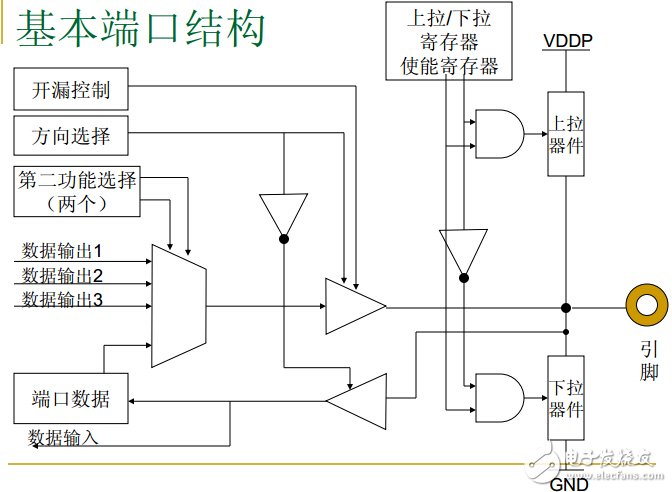
(3) Port-related registers
- PX_PUDSEL Pull-up/Pull-down selection register
-PX_PUDEN Pull-up/Pull-down Enable Register
-PX_OD Open-drain control register
- PX_DIR direction register (P2 port can only be used as input)
- PX_ALTSEL0 Secondary function selection register 0
-PX_ALTSEL1 Second function selection register 1
- PX_DATA Port data register
The X in PX is the port number. The registers are all 8 bits, and each bit corresponds to a pin.
I2C bus and SPI bus
The I2C bus and SPI bus are both "bit synchronous" serial interfaces, but they have some differences:
nn The data signal of the I2C bus requires: start, stop and ACK signals, requiring the other party to respond
I2C bus circuit link
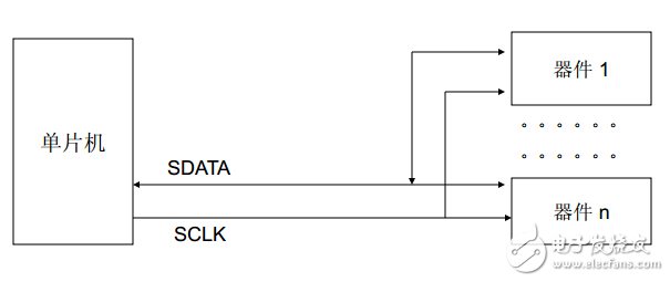
SPI bus: two serial data lines and one clock line. The data lines are divided into output and input. For multiple chips, a chip select CS is also required.
SPI bus structure

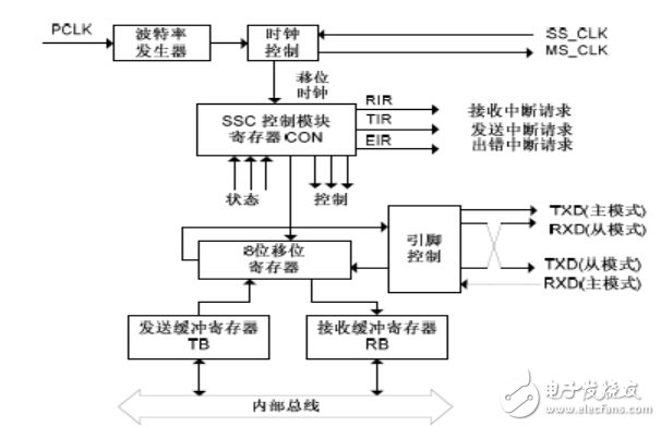
XC866 SSC
XC866 has a high-speed synchronous serial channel SSC, which is compatible with SPI and 8051 serial port mode 0;
- Baud rate is independently programmable: it has a dedicated 16-bit baud rate generator with reload function;
-Data width is specified as 2 to 8 "characters";
- LSB can be sent first (compatible with 8051 serial mode 0) or MSB can be sent first (compatible with SPI);
-Data can be shifted on the rising or falling edge of the clock;
-Can generate shift clock or receive shift clock;
- The names are different: MOSI=MTSR, MISO=MRST;
SSC block diagram
Digital-to-Analog Converter (DA)
working principle
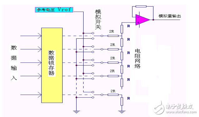
DA converter chip
The main components of the DA converter are the resistor network and the corresponding analog switch array. [page]
Analog output is usually current output. The operational amplifier in the figure converts the current output into voltage output. The feedback resistor is connected according to the manufacturer's design. The output voltage and the reference voltage satisfy the following relationship:
Vout= - Vref X (data / (2n-1))
Among them: n is the number of bits of the digital quantity, data is the input digital quantity. Some chips have their own data latch and provide their own reference voltage. There are many types of chips, and the most common ones are DAC0832.
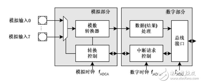
AD Converter
- Successive approximation
-8-bit or 10-bit accuracy, 8 analog channels
- 4 independent result registers
- Single conversion and auto scan function
- Programmable sampling clock and programmable clock divider
-Integrated sample and hold circuit
-Data compression filtering
-Flexible interrupt generation mode, configurable interrupt service nodes
- The ADC module can be turned off to reduce power consumption
XC866 AD converter block diagram
AD conversion initialization explanation
AD converter initialization procedure:
-SFR_PAGE(_ad0, noSST); // switch to page 0
-ADC_GLOBCTR = 0x70; // f32, 8-bit width
-ADC_PRAR = 0x94; // Set arbitration mode and priority
- SFR_PAGE(_ad1, noSST); // switch to page 1
-ADC_QMR0 = 0x00; // ADC mode, disable external trigger
-ADC_CRMR1 = 0x01; // ADC mode, enable request source
-SFR_PAGE(_ad0, noSST); // switch to page 0
-ADC_GLOBCTR |= 0x80; // Enable analog part
- XC866's ADC uses 7 pages of SFR, each page occupies addresses CAH~CFH and D2H, D3H. Different pages have different contents, and D1H is used as a paging register to determine which page to use. GLOBCTR and PRAR are on page 0, and QMR0 and CRMR1 are on page 6.
Programmable Counter Array PCA and Capture Compare Unit CCU
Enhanced timer/counter module, or a combination of multiple modules, called PCA/CCU
- Timer clock can be selected: another timer overflow or fixed divider output
- Multiple functions can be selected, such as capture/compare/reload/PWM output, etc.
- Multiple capture/compare/reload data registers to form multiple PWM outputs
- Capture/overflow/match can generate interrupt
- A separate reload register can set the PWM period
Capture compare unit CCU6 of XC866
The capture/compare unit 6 (CCU6) has two independent timers (T12, T13) that can be used to generate pulse width modulation (PWM) signals, which are particularly suitable for controlling AC motors. CCU6 also supports some special control modes for block switching and multi-phase motors.
The three channels of timer T12 can work in capture and/or compare mode. Timer T13 can only work in compare mode.
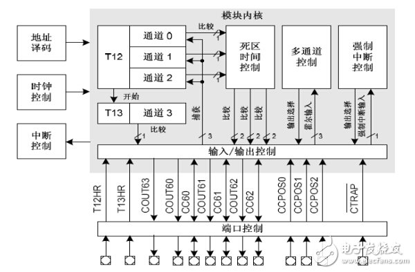
The output sequence generated by the multi-channel control unit can be modulated by T12 and/or T13. The modulation sources can be selected and used in combination.
Timer T12, T13 characteristics:
-Timer T12 Features:
1. 3 capture/compare channels, each channel can be used as a capture or compare channel
2. Supports three-phase PWM generation (6 outputs, each signal corresponds to the upper bridge arm or lower bridge arm switch)
3. 16-bit precision, maximum counting frequency = peripheral clock frequency
4. Single channel dead time control to avoid power stage short circuit
5. Synchronously refresh T12/T13 registers
6. Generate center-aligned and edge-aligned PWM
-Timer T13 Features:
1. Single comparison channel, single output
2. 16-bit precision, maximum counting frequency = peripheral clock frequency
3. Can be synchronized with T12
A brief introduction to three-phase motor PWM generation
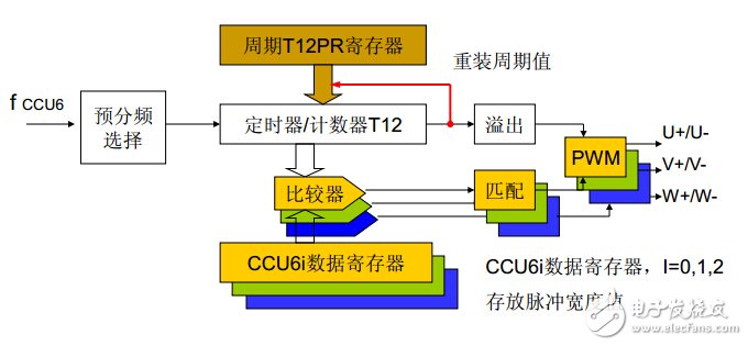
The different pulse width values of the three phases need to be written into the CCU6i mapping register CCU6iSR in real time
The three-phase outputs U, V, and W are output through the CCU6i and COUT6i pins in pairs, with opposite polarities.
Various settings: clock selection, pre-scaling selection, dead time, output pin configuration, and multiple mode selections are briefly discussed here.
Three-phase motor SPWM signal principle
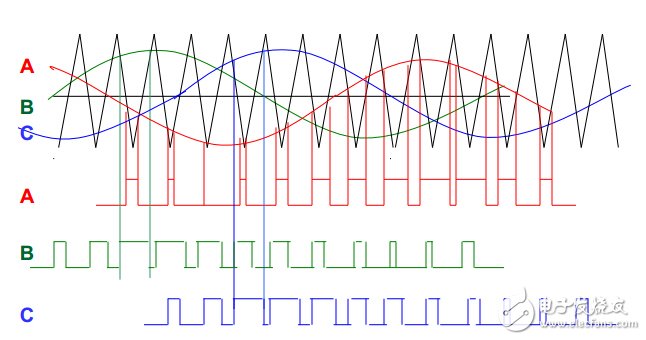
The triangle wave is called the "carrier wave" and the sine wave is called the "modulation wave". The phase difference between A, B, and C is 120 degrees. Their SPWM waveform parameter tables are actually the same, but they also differ by 120 degrees.
The SPWM waveform parameter table is actually the corresponding pulse width in each triangle wave cycle.
Three-phase motor/brushless motor control example
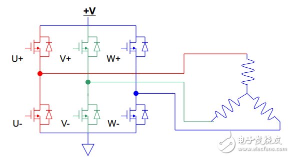
The U+/U-; V+/V- and W+/W- outputs of the microcontroller CCU6 are connected to the IGBT after being driven.
Changing the cycle and pulse width in real time can achieve the purpose of frequency conversion and adjust the output power, thereby controlling the motor speed.
Engineers' questions and answers about the use of XC866:
(1) Which IDE should I choose for XC866?
A: "Miniwigger + KEIL V3 cracked version
keil for c51 v8
Infineon DAVE V2.1
infineon memtool v4.01.05
fload Downloader"
(2) I want to use Proteus to simulate Infineon's XC866, but it is not in the component library. What should I do?
A: "Since there is no Infineon MCU in the Proteus component library, it is difficult to make it yourself. If it is other commonly used devices, find a similar one to replace it. You can use miniwager, which is Infineon's own simulator, or you can use Nanjing Weifu's Multi-Infineon simulator."
(3) SCLK clock problem in Infineon XC866
Q: The SSC has been set in DAVE, but when I finished programming and simulated in Keil, I found that SCLK was always 0. Can't XC866 generate clock signals after the SSC is set?
A: "The built-in SPI peripheral will only output a clock when sending data."
(4) XC866 MBC level OCD mode help
Q: xc866 development board. Use ulink to debug through ocds interface. The book says: If (MBC, TMS, P0.0) = (0, 1, 1), it will enter OCDS mode to debug the program code. First initialize OCDS, then jump to address 0000H of the program memory, execute the user code in Flash or ROM memory, and start debugging. In OCDS mode, the lower 64 bytes of the internal data memory (address 00H-3FH) can be selected to be mapped as 64 bytes of monitoring RAM or internal data RAM.
Why is the MBC pin always high when debugging with ulink? It is different from what is said in the book. I checked it with a multimeter. Could it be that MBC is set to low level for a moment, enters OCD mode, and then sets it high again?
When using xc800_fload to burn the program, the MBC pin must be connected to the ground, otherwise it cannot be burned.
A1: "(MBC, TMS, P0.0) = (0, 1, 1) refers to the level of these pins after the chip is reset. After reset, xc866 will automatically detect the level of these three pins to determine whether the chip enters download mode, JTAG mode, or runs the program. For your question
1. OCDS mode: Your understanding may be correct, because MBC, TMS, P0.0 are all connected to Ulink, so I guess the actual process is like this, Ulink first sets MBC, TMS, P0.0 to 0, 1, 1. Then reset the chip (Ulink pulls down Reset), release the reset chip, and then the chip enters OCDS mode.
2. If MBC = 0 and TMS = 0, the chip will enter BSL mode after reset and perform serial port download (via FLoad)"
A2: In other words, when the debug button is clicked in the Keil software interface under the ulink connection, ulink will first reset the chip, and then set MBC, TMS, P0.0 to (0, 1, 1) to let the chip enter the ocds mode. After entering the mode, the settings of MBC, TMS, and P0.0 will be restored to the normal mode. In this way, for example, when debugging at a breakpoint, after manually pressing the reset button, the chip can enter the normal running mode, and the program will run normally instead of entering the ocds mode again.
As for fload mode, from the circuit point of view, MBC can only be controlled by the OCDs signal of ulink, so it is necessary to manually increase the low level, and the program cannot run after burning.
Previous article:Public Transportation IC Card Data Collection System Based on Wi-Fi Technology
Next article:Application of AT89C2051 in the external display screen of money counting machine
- Popular Resources
- Popular amplifiers
 Professor at Beihang University, dedicated to promoting microcontrollers and embedded systems for over 20 years.
- LED chemical incompatibility test to see which chemicals LEDs can be used with
- Application of ARM9 hardware coprocessor on WinCE embedded motherboard
- What are the key points for selecting rotor flowmeter?
- LM317 high power charger circuit
- A brief analysis of Embest's application and development of embedded medical devices
- Single-phase RC protection circuit
- stm32 PVD programmable voltage monitor
- Introduction and measurement of edge trigger and level trigger of 51 single chip microcomputer
- Improved design of Linux system software shell protection technology
- What to do if the ABB robot protection device stops
- Huawei's Strategic Department Director Gai Gang: The cumulative installed base of open source Euler operating system exceeds 10 million sets
- Download from the Internet--ARM Getting Started Notes
- Learn ARM development(22)
- Learn ARM development(21)
- Learn ARM development(20)
- Learn ARM development(19)
- Learn ARM development(14)
- Learn ARM development(15)
- Analysis of the application of several common contact parts in high-voltage connectors of new energy vehicles
- Wiring harness durability test and contact voltage drop test method
- [AT-START-F425 Review] + Transplanting u8g2 monochrome graphics library to drive 0.96-inch OLED
- One of the outstanding achievements in the field of communications: scattering communications
- ALLEGRO PROBLEMS
- [TI recommended course] #TI? Application of interface chips in automotive products#
- [NXP Rapid IoT Review] + Use of Bluetooth (1 Preliminary Exploration)
- 500 yuan for infrared counting microcontroller
- EE mobile station development board introduction: STM32 Nucleo Pack FOC and 6 step motor control (ST 3-phase motor...
- TI NIR SCAN NANO Consulting
- Why can the serial port receive 9600 but lose bytes at 115200?
- What is the chip with 4BMN silk screen? It has 5 pins.

 5962F9678501VPA


 京公网安备 11010802033920号