1 Introduction to TDA5210 Receiver Chip
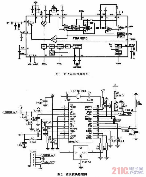
TDA5210 is a low-power, single-chip FSK/ASK superheterodyne wireless receiver chip, with an operating frequency band of 810-870 MHz and 400-440 MHz. The chip is highly integrated and only requires a small number of peripheral devices to complete the application. Its pins are compatible with Infineon's ASK receiver TDA5200. The TDA5210 chip has built-in low-noise amplifier (LNA), double-balanced mixer, voltage-controlled oscillator (VCO), phase-locked loop (PLL), crystal oscillator, limiter, phase-locked loop FSK demodulator (PLLFSK dcmodulator), data filter, data limiter, peak detector and other circuits. At the same time, it also has an automatic sleep function to reduce battery consumption and is suitable for occasions with high power consumption requirements. Figure 1 is the internal block diagram of TDA521 O.
[page]
2 Schematic Design
The schematic diagram of the receiving module is shown in Figure 2. The filtering network composed of C1, C2, L1, and C3 matches the wireless signal at the antenna end and sends the weak signal within the bandwidth frequency range to the LIN pin; after the signal is amplified by the LNA (low noise amplifier) inside the chip, it enters the MI pin and mixes with the signal generated by the VCO to separate the data signal from the high-frequency signal, and then passes through a 10.7 MHz ceramic intermediate frequency filter, and then passes through the internal limiter LIMITEB. Finally, the signal is separated by a comparator to generate the final data level signal.
3 PCB (printed circuit board) design and device selection
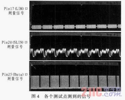
In general applications, for the convenience of design and to reduce the interference of the system to the wireless receiving circuit, the receiving module appears in the form of an independent module, and its physical size is generally small, which requires that the arrangement of components should be as compact as possible during PCB wiring, and the routing distance between components should be as short as possible to reduce signal interference. In addition, the antenna is crucial to the module's reception effect. Therefore, when routing, the copper foil antenna part on the PCB should be routed as close to the edge of the PCB as possible and away from the interference source crystal oscillator and intermediate frequency filter, which can improve the module's reception effect. The actual picture of the receiving module PCB is shown in Figure 3.
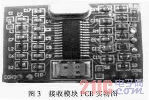
The parameter selection of key components is crucial for the reception of wireless signals. Therefore, selecting components with appropriate parameters can improve the reception effect of the receiving module and reduce noise. TDA521O is a narrowband RFIC. The deviation of the crystal oscillator and the inconsistency of the crystal oscillator load capacitance will affect the receiving sensitivity. It is recommended to use specifications of 13.401 55 MHz, a frequency deviation of 10 ppM, and a load capacitance of 12 pF. The intermediate frequency filter also has a great influence on the receiving effect. Its main parameters are: center frequency, 3 dBbandwidth, etc. The center frequency needs to be 10.7 MHz; 3 dB bandwidth should be selected (150±50 kHz). If the bandwidth parameter is selected too small, the signal within the normal range of the center frequency cannot pass through, affecting the receiving distance. If the bandwidth is selected too large, a large amount of wireless noise will be generated. In extreme cases, the noise will even drown out the normal signal. In addition, the quality of the capacitor and inductor at the back end of the antenna is also very important. It is recommended to choose a device brand with relatively high quality.
4 Hardware debugging
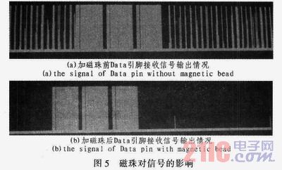
According to the internal structure of TDA5210, module debugging can be based on the direction of the received signal, and the oscilloscope can be used to measure the signal at each key point in the signal direction to determine whether the device circuit of each part is working properly, and adjust the device parameters of the corresponding part to improve the output strength of the signal. You can test Pin17 (LIM), Pin 20 (SLIN), Pin 25 (DATA) in turn, and the basic waveform of the signal of each key measurement point and each pin is shown in Figure 4.
[page]
During the debugging process, it was found that the Data pin of TDA521O, which outputs the demodulated data signal, would output a lot of noise in the idle state. These noise signals are very unfavorable for the reception and processing of the main control microcontroller. After analysis, the noise is caused by the interference generated by the crystal oscillator or other high-frequency components of the MCU in the main control board. These interferences are crosstalked to the receiving board through the power supply and ground wires. Therefore, to solve this problem, a 500 Ω magnetic bead can be connected to the power supply and ground terminals of the receiving board to suppress high-frequency crosstalk. Figure 5 shows the signal output after adding the magnetic bead.
As can be seen from Figure 5, after adding the magnetic beads, the noise is suppressed and the receiving effect is significantly improved.
5 Wireless module application
5.1 System block diagram
The wireless intelligent access control system uses a wireless receiving module based on TDA5210, as shown in Figure 6. The system main control chip uses Freescale MC68HC908JK8. The microcontroller has 8 K programmable Flash memory, 256 bytes of RAM on-chip memory, 2 16-bit timers, 13 A/D input channels, and input signal capture, PWM output and other functions. At a working voltage of 5 V, the maximum bus frequency can reach 8 MHz. At the same time, it has high electromagnetic compatibility performance and is suitable for systems with high requirements for electromagnetic interference.
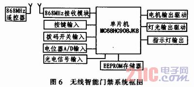
The input part of the system includes: receiving wireless signal input, key input, dip switch input, potentiometer A/D input, and photoelectric signal input. The drive output part of the system includes motor drive output, light drive output, and indicator light output.
The data encoding chip on the remote control side uses Microchip HCS301. HCS301 is an encoding chip based on Keelog rolling code technology. Compared with fixed encoding chips, it has high system security performance and is very suitable for occasions with high security requirements. The system memory uses ATMEL's EEPROM AT24C02 chip.
5.2 System software design
The receiving end of the main control board does not use Microchip's keelog hardware decoding chip HCS512, but uses software decoding, which not only increases the flexibility of software control, but also reduces the cost of the system. The level pulse signal output from the wireless receiving module is connected to the external interrupt port of the microcontroller, and the control program decodes it according to the data pulse width level specification of HCS301. The main control program controls the door according to the key information sent by the remote control.
AT24C02 is used to save the ID number of the learned remote control transmitter chip to ensure the corresponding relationship between the main control board and the remote control. A main control board can store multiple sets of remote control information, and can achieve a one-to-one or one-to-many correspondence according to user needs. The main control chip can run in different modes according to the state combination of the dip switch. At the same time, according to the photoelectric signal input, the main control chip can detect whether there is a person or object passing under the door to avoid accidents caused by people or objects being pressed by mistake. The potentiometer is used to generate different A/D values, and different A/D values correspond to different time positions, thereby controlling the switch travel of different types of doors. In addition to being controlled by the remote control, the system can also be controlled by pressing the buttons on the main control board.
Compared with the systems using 315 MHz and 433 MHz, the wireless intelligent access control system using the 868 MHz frequency band has fewer interference sources. At the same time, the wireless control system based on the TDA5210 receiving module has high sensitivity and anti-interference performance.
6 Conclusion
This paper describes the design of 868 MHz wireless receiving module based on Infineon TDA5210 circuit, details the method of signal debugging, analyzes the cause of high-frequency noise, and proposes a method of signal suppression. It also analyzes its application in the intelligent access control system, which has been mass-produced and is very stable.
Previous article:Design of LED lighting drive circuit based on SA7527
Next article:Application of three-phase SPWM generator HEF4752 in variable frequency speed regulation system
 Professor at Beihang University, dedicated to promoting microcontrollers and embedded systems for over 20 years.
- Innolux's intelligent steer-by-wire solution makes cars smarter and safer
- 8051 MCU - Parity Check
- How to efficiently balance the sensitivity of tactile sensing interfaces
- What should I do if the servo motor shakes? What causes the servo motor to shake quickly?
- 【Brushless Motor】Analysis of three-phase BLDC motor and sharing of two popular development boards
- Midea Industrial Technology's subsidiaries Clou Electronics and Hekang New Energy jointly appeared at the Munich Battery Energy Storage Exhibition and Solar Energy Exhibition
- Guoxin Sichen | Application of ferroelectric memory PB85RS2MC in power battery management, with a capacity of 2M
- Analysis of common faults of frequency converter
- In a head-on competition with Qualcomm, what kind of cockpit products has Intel come up with?
- Dalian Rongke's all-vanadium liquid flow battery energy storage equipment industrialization project has entered the sprint stage before production
- Allegro MicroSystems Introduces Advanced Magnetic and Inductive Position Sensing Solutions at Electronica 2024
- Car key in the left hand, liveness detection radar in the right hand, UWB is imperative for cars!
- After a decade of rapid development, domestic CIS has entered the market
- Aegis Dagger Battery + Thor EM-i Super Hybrid, Geely New Energy has thrown out two "king bombs"
- A brief discussion on functional safety - fault, error, and failure
- In the smart car 2.0 cycle, these core industry chains are facing major opportunities!
- The United States and Japan are developing new batteries. CATL faces challenges? How should China's new energy battery industry respond?
- Murata launches high-precision 6-axis inertial sensor for automobiles
- Ford patents pre-charge alarm to help save costs and respond to emergencies
- New real-time microcontroller system from Texas Instruments enables smarter processing in automotive and industrial applications
- Msp430 contains ADC12 module
- A wrong partner will bury your genius ideas
- Automatic air conditioning comes in
- Solution to CCS8.1.0 not finding .h files
- EEWorld invites you to attend the 2019 STM32 Summit and Fan Carnival!
- Ask a question about the LM35CZ temperature sensor
- Functions of vent valve and drain valve of magnetic flap level gauge
- FatFs transplantation based on SPI for MSP430F5438A microcontroller
- Problem with STM32F767 timer overflow interrupt flag
- Comparison of the advantages of digital cameras and analog cameras in machine vision system design

 USB Development Encyclopedia 4th Edition


 京公网安备 11010802033920号