Understanding TSV in one article

Publisher:QuailLatest update time:2022-05-09 Source: 迈铸半导体 作者:Dr. GuKeywords:TSV Reading articles on mobile phones Scan QR code
Read articles on your mobile phone anytime, anywhere

In the first month of 2000, Professor Sergey Savastiou of Santa Clara University published an article titled "Moore's Law – the Z dimension" in the journal Solid State Technology. The title of the last chapter of this article is Through-Silicon Vias, which is the first time that the term Through-Silicon Via has appeared in the world. The time when this article was published seems to indicate that in the new millennium, TSV is destined to have its extraordinary performance.
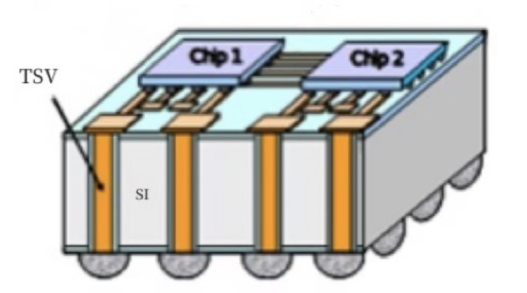
image.png

TSV schematic diagram


TSV is the abbreviation of Through-Silicon Via, which is a vertical electrical interconnection passing through the silicon substrate.


If wire bonding and flip-chip bumping provide electrical interconnection between the chip and the outside, and RDL (rewiring) provides electrical interconnection in the horizontal direction inside the chip, then TSV provides electrical interconnection in the vertical direction inside the silicon wafer. As the only vertical electrical interconnection technology, TSV is one of the core technologies of advanced semiconductor packaging.


Vertical interconnection was born with integrated circuits
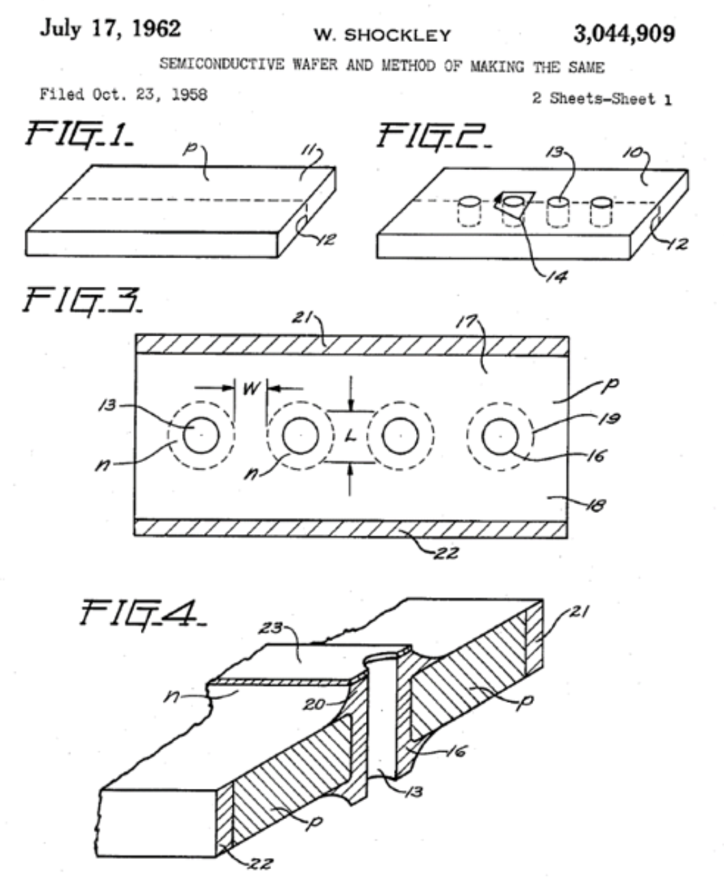

In the fall of 1958, William Shockley sat in his office thinking about how to design transistors for high-frequency applications. As early as 1947, he developed the first transistor with Bardeen and Brattain, and won the Nobel Prize together in 1956.

"Why can't you just punch some holes in the wafer?" Shockley muttered to himself.
Soon Shockley applied for a patent - (SEMICONDUCTIVE WAFER AND METHOD OF MAKING THE SAME), which was the first patent in history to etch through holes on a wafer. Although the original intention of this patent was only for the application of transistors in the high-frequency field, in this patent, Shockley also mentioned that conductive metal could be filled in the through hole if necessary. In this way, the person who invented the transistor also became the first person to think of making conductive holes in the wafer. Another major event happened in the same year. The integrated circuit (chip) that made multiple transistors together was also invented.
image.png
Schottky's patent for making holes in silicon wafers

Since then, IBM has begun to focus on the field of integrated circuits and has made breakthroughs in vertical electrical interconnection.

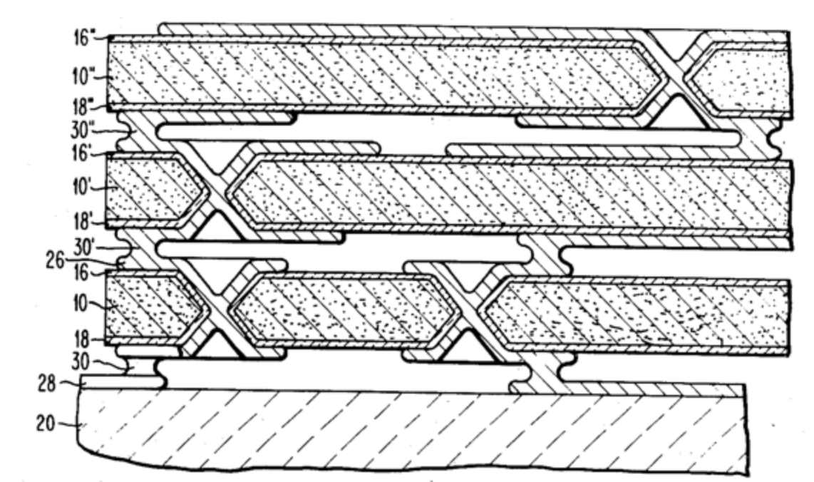
Six years later, in 1964, IBM applied for a patent (METHODS OF MAKING THRU-CONNECTIONS IN SEMICONDUCFOR WAFERS), proposing to use degenerate doping in through holes to reduce resistance to achieve vertical interconnection of silicon wafers, that is, to use low-resistance silicon as the conductive material. However, this patent only stayed at the upper and lower surface devices of the silicon wafer itself, and was not used for stacking multiple chips. It was not until five years later in 1969 that IBM first proposed the stacking of multi-layer chips based on vertical interconnection in another patent (HOURGLASS-SHAPED CONDUCTIVE CONNECTIONTHROUGH SEMCONDUCTOR STRUCTURES), as shown below:

image.png
The first chip stacking patent

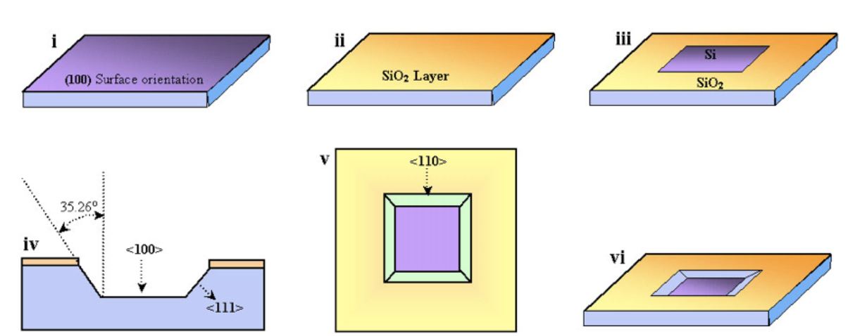
It seems that it took only 11 years, even before the term TSV was officially invented, for the concept and process of vertical interconnection to be developed. However, this IBM patent has not been widely used. The reason is that the shape of the via in this patent, as indicated by its patent name "HourGlass", is hourglass-shaped, which takes up too much area. This shape of via is related to a discovery made by HA Waggener of Bell Telephone Laboratories two years ago (1967): KOH has a huge difference in the etching rate of different crystal planes of single crystal silicon [1].

For example, the corrosion rate of the <100> crystal plane is hundreds of times greater than that of the <111> crystal plane. This feature can be used to easily etch through holes in the commonly used <100> silicon wafer, but the hole shape is an inverted pyramid (or hourglass shape). With the continuous development of Moore's Law, transistors per unit area are becoming more and more dense, and this vertical interconnection that occupies a large surface area has obviously lost its meaning.

image.png
Schematic diagram of KOH etching

But perhaps influenced by the stacked chip concept proposed by IBM, the idea of ​​3D integrated chips spread like wildfire in the semiconductor industry. Since then, more than 40 research institutions and companies have participated in the research of related technologies [2]. As the core technology of 3D stacked chips, vertical electrical interconnection has naturally attracted much attention. In the following 1970s to 1990s, many breakthroughs in semiconductor micromachining technology laid a solid foundation for the birth of modern TSV.

Technological breakthrough


As a semiconductor material, silicon has neither good conductivity nor good insulation. To achieve vertical electrical interconnection on a silicon wafer, it is generally necessary to make micropores on it (depending on the specific application, the pore size is generally from a few microns to hundreds of microns, a hair is about 50 microns, and the number of pores required on a single silicon wafer can reach hundreds of thousands); deposit insulating materials on the sidewalls of the pores; fill the micropores with conductive materials, and other manufacturing steps. The most challenging of these is the batch etching and conductivity of micropores.
First of all, it is not easy to process micropores on silicon wafers. Silicon is hard and brittle, and the apertures that need to be processed are small and large, so it is simply not feasible to use traditional mechanical processing methods. In Schottky's patent in 1958, he proposed to use the difference in chemical corrosion rate at the interface of the crystal material to achieve micropore etching (due to the long history and lack of sufficient information, it is not possible to fully understand Schottky's corrosion method*_*).

Reverse sputtering (i.e., plasma physical bombardment etching) has also been tried for etching, but the rate is too slow, so people have to go back to the old way of chemical etching. The KOH etching mentioned above is a type of chemical etching, which is anisotropic etching, but it cannot achieve the cylindrical holes that are most suitable for TSV. Since the 1980s, Japan has begun to focus on three-dimensional integration and established the "Three-Dimensional Circuit Element R&D Project". In 1983 and 1984, Hitachi's two patents mentioned the use of laser drilling to solve the problem of micro-hole etching on silicon wafers [3]. Unlike the "hourglass holes" of KOH etching, these patents all use cylindrical holes. However, laser processing also has many problems. On the one hand, the holes can only be processed one by one, which is time-consuming. On the other hand, the processed holes have problems such as rough surface and edge collapse. It was not until the 1990s that silicon etching ushered in a breakthrough, and DRIE deep silicon etching technology was born.

DRIE, the acronym for Deep Reactive Ion Etching.

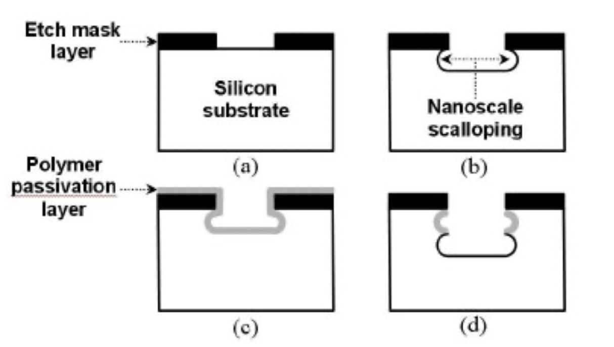
This technology is a high aspect ratio silicon etching technology developed by Robert Bosch in Germany in 1994 based on a previous low-temperature ion silicon etching technology [4]. This technology uses a very clever method to achieve isotropic etching to etch cylindrical holes. Isotropic etching is different from the anisotropic etching of KOH mentioned above. It etches silicon wafers uniformly in all directions, so under normal circumstances it can only etch spherical holes on silicon wafers. The core idea of ​​using isotropic etching to achieve cylindrical hole etching is to divide the etching into countless small steps.

The specific method is: first expose the silicon where the micropores need to be etched on the silicon wafer, etch a thin layer on the silicon wafer with isotropic corrosive gas, then deposit a protective layer on the surface of the etched pit, then use plasma to knock off the protective layer at the bottom of the pit, and then etch a thin layer with isotropic corrosive gas. Through multiple such tiny isotropic etching cycles, batches of high aspect ratio micropores can be etched on the silicon wafer. In fact, this technology is so important that it later became the core manufacturing technology of MEMS.

image.png
Schematic diagram of DRIE

Conductivity of micropores is also challenging. In 1958, Xiao Lao's patent only mentioned the idea of ​​filling metal in the hole, but did not provide any specific implementation method; in 1964, IBM's patent used degenerate doping to reduce the resistance of silicon and thus transform silicon itself into a conductive medium. This method cannot be used for the conductivity of micropores; and in the patent applied by IBM in 1969, the metal layer was achieved by sputtering. Although sputtering was the mainstream metal deposition method for semiconductors at the time, sputtering can generally only be used for thin metal deposition with a thickness of less than 1um, and has poor coating properties, so it can only be used for the metallization of hourglass-shaped holes.
In 1970, Hitachi first proposed in a patent that metal deposition would be achieved in semiconductor wafers by electroplating [5]. Although the electroplating in this patent was only for the purpose of achieving ohmic contact between metal and silicon, this research opened the prelude to the use of electroplating in semiconductor processing. Electroplating technology is a brand-new metal forming technology invented by British and Russian scientists in the first half of the 19th century. It is different from all the purely physical metal processing methods that humans have used before, such as forging, casting, evaporation deposition, sputtering deposition, machining, etc. Electroplating is an electrochemical technology. This technology was initially mainly used for the mass production of metal artworks. Because of its relatively fast deposition speed and the ability to achieve mass deposition, the electroplating technology finally came together with semiconductors more than 100 years after its invention.
Five years later, in 1975, IBM further combined X-ray lithography with electroplating and began to explore the use of electroplating for the deposition of thick metals on wafers [6].
In 1982, this technology was further developed into an important MEMS technology in Germany, LIGA. The full name is Lithographie, Galvanoformung, Abformung (English: Lithography, Electroplating, and Molding) [7]. This is a technology that combines photolithography and electroplating for the deposition of high aspect ratio metal structures. As the core technology of MEMS (micro-electromechanical systems), LIGA has made a lot of contributions to the early development of MEMS. If you still remember the above, DRIE deep silicon etching later became the core technology of MEMS. So it is not an exaggeration to say that TSV and MEMS are twin brothers in technology!
In the mid-1990s, a major event occurred in the semiconductor industry: IBM used copper electroplating Damascus process to completely replace sputtered aluminum as transistor interconnects in integrated circuits. In this way, copper electroplating began to become a standard process in the semiconductor industry, making it more logical to use copper electroplating for TSV micro-hole metallization filling.
At this point, the two core technologies of modern TSV: deep silicon etching and electroplating have emerged.

Going commercial

[1] [2]
Keywords:TSV Reference address:Understanding TSV in one article

Previous article:Researchers develop wood-derived nanocellulose paper semiconductors
Next article:Researchers can now measure the 'wettability' of graphene and other 2D materials at the molecular level

Recommended ReadingLatest update time:2024-11-16 12:27

Understanding TSV in one article
In the first month of 2000, Professor Sergey Savastiou of Santa Clara University published an article titled "Moore's Law – the Z dimension" in the journal Solid State Technology. The title of the last chapter of this article is Through-Silicon Vias, which is the first time that the term Through-Silicon Via has ap
[Semiconductor design/manufacturing]
Understanding TSV in one article
Latest Semiconductor design/manufacturing Articles
Change More Related Popular Components

EEWorld
subscription
account

EEWorld
service
account

Automotive
development
circle

About Us Customer Service Contact Information Datasheet Sitemap LatestNews


Room 1530, 15th Floor, Building B, No.18 Zhongguancun Street, Haidian District, Beijing, Postal Code: 100190 China Telephone: 008610 8235 0740

Copyright © 2005-2024 EEWORLD.com.cn, Inc. All rights reserved 京ICP证060456号 京ICP备10001474号-1 电信业务审批[2006]字第258号函 京公网安备 11010802033920号