1 Working principle of controller
The upper computer of the galvanometer laser marking controller is a computer with marking software installed. The text and graphics are processed into a large amount of marking data through image processing, and the effect diagram is displayed on the marking software interface. The marking data is transmitted to the extended memory RAM by the USB bus, and then taken out by the DSP in sequence and sent to the D/A conversion chip. After conversion, the D/A chip outputs an analog voltage of -5 to 5 V to drive the scanning galvanometer and control the power of the laser power supply. A GPIO (general input/output) pin controls the switch of the laser energy. The x and y axis galvanometers control the laser focus to move orderly on the two-dimensional plane to complete various forms of text and graphic marking.
2 Hardware circuit design of galvanometer laser marking controller
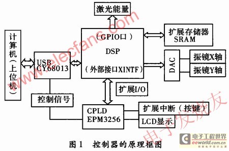
The principle block diagram of the system is shown in Figure 1. The galvanometer laser marking controller mainly includes USB communication circuit, expansion memory circuit, D/A conversion circuit and CPLD circuit.

2.1 USB communication interface
The USB communication module uses Cypress's CY7C68013. There are two ways to connect USB and DSP: FIFO and GPIF. In this system, FIFO is used, and the read and write signals are provided by CPLD and DSP. The SLOE of the USB chip is connected to the external interrupt of the DSP. Other control signals are decoded by the DSP through the CPLD and connected to the USB chip. The data line and two address lines of the DSP are directly connected to the USB.
2.2 High-speed D/A conversion circuit
The digital-to-analog conversion part is the key part of the controller. This system requires three D/A channels to control the x-axis and y-axis of the galvanometer and the laser power respectively. The main technical parameters of AD7836 in this system meet the requirements:
(1) Single-chip 4-channel 14-bit D/A conversion; (2) Voltage output, the maximum voltage output range is ±10 V; (3) The output voltage settling time is typically 16 μs.
The D/A voltage resolution is: 5 V/213 = 0.61 mV. Compared with bipolar and unipolar voltage outputs, the circuit omits the operational amplifier that changes the voltage polarity, making the circuit simpler.
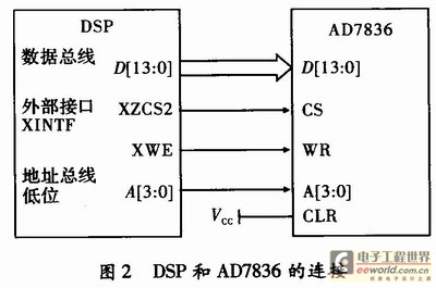
Ad7836 supports interfaces with microprocessors and DSPs above 16 bits, including 14-bit data lines, 3-bit address lines A0, A1, A2, and control signals CS, CLR, WR, and SEL. When CS is at a low level, AD7836 is selected; only when CLR is at a high level can the internal data register value of the D/A converter control the analog voltage output value; WR is valid at a low level and can be combined with CS to write data into the input buffer. When SEL is at a high level, the user-set register E value is output to VOUT, so it can be grounded. When the system is working, due to the use of the external interface XINTF, the operation of the D/A chip is the same as reading and writing data from SRAM. The starting address of the external interface 2 area that controls the D/A chip is 0X08 0000. The corresponding value can be changed at any time in the program to control the voltage value of the D/A conversion, and then control the position of the marking point. If you want to mark a picture, you can output the position of each marking point and the laser energy in a line-by-line scanning manner.
The pin connection between DSP and AD7836 is shown in Figure 2.

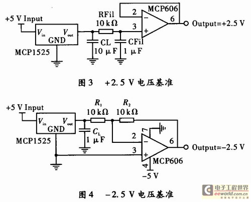
Since the driving voltage range of the galvanometer used is also ±5 V, the reference voltage VREF(+) and VREF(-) of each channel in this system are connected to ±2.5 V respectively. The precise ±2.5 V reference voltage uses Microehip's dedicated 2.5 V voltage reference source MCPl525 and OP operational amplifier MCP606 in the hardware circuit design. As shown in Figure 3, after the +2.5 V voltage reference is generated by MCPl525, in order to reduce noise, RC low-pass filtering and MCP606 are used. Here, MCP606 is used as a voltage follower. As shown in Figure 4, the -2.5 V voltage is generated by +2.5 V through a voltage divider composed of two equal resistors and MCP606.

The pin voltages of AD7836 and DSP are different, so they cannot be directly connected. The SN74ALVCl64245 chip is selected in the system to isolate the data buses on both sides. Its output enable control pins OE1 and OE2 are both connected to low level, and the direction of the data line DIR1 and DIR2 are both connected to high level to ensure that the chip output changes instantly with the input.
2.3 Extended Data Storage
The memory is used to temporarily store the marking data transmitted from the host computer. The external expansion memory uses IS61LV51216, which is a 512 kB, 16-bit SRAM memory with a total of 19-bit address bus and 16-bit data bus. In this system, the SARAM access time is 10 ns, CMOS process, 3.3 V power supply, input and output are TTL compatible, and it is suitable as an external expansion memory for DSP. The memory is extended through the external interface XINTF of DSP, and the /XZCS6AND7 pin of F2812 is used as the chip select, so it corresponds to the external interface 6 area of the memory map, and the address range is 0X10 0000~0X17FFFF.
2.4 CPLD System
The CPLD in this system uses the EPM3256A chip of the MAX3000A series of Altera, and the firmware of the CPLD is designed with the software MAX+plusII. The CPLD is mainly used to control the data transmission of the USB chip, and it is expanded to the interrupt button and LCD display module. In addition, the DSP system reserves multiple GPIO interfaces, which can control the multi-dimensional motion control platform composed of stepper motors. By reserving GPIO ports and using CPLD chips, the scalability of the system is enhanced.
3 Controller system software development
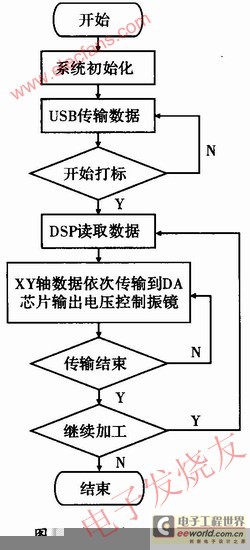
The control system software consists of two parts. The upper computer is designed with the visual object-oriented language VB 6.0, which is mainly responsible for the generation and packaging transmission of marking data, as well as the user interface to achieve human-computer interaction; the lower computer DSP is written in C/C++ and developed with the efficient C compiler and integrated development environment provided by TI: Code Studio (CCS). The main flow chart of the control system is shown in Figure 5.

After the marking machine is turned on, the lower computer program initializes each chip and memory according to the parameters on the user interface. The parameters include laser energy, number of scans, text filling method, etc. Then wait for the upper computer to transmit the marking data through the USB interface, and the marking data is first saved in the data memory. At this time, no matter whether the marking start command is issued from the user interface or the keyboard, the DSP takes out the marking data from the data memory and sends it to the D/A chip. The D/A chip outputs the corresponding voltage to drive the galvanometer until the marking is completed. The same marking pattern only needs to transmit data once, and select the start processing button from the software or keyboard.
When marking graphics, the graphics file is imported and processed, and then converted into marking position data; when marking text, the Windows API function GetGlyphOutline is called in VisualBasic to obtain the outline of the text, which can be scaled, rotated, etc. without affecting the text display quality, and the display effect is displayed on the user interface through the DrawGlyph function. Figure 6 shows the display effect of Chinese characters in the software user interface.

4 Conclusion
This paper introduces a laser marking controller based on TMS320F2812 DSP. It uses a 4-channel output D/A converter to control the galvanometer and laser power supply. The high-performance D/A conversion module greatly improves the speed and accuracy of laser marking. The USB interface makes the marking controller plug-and-play and improves the stability of data transmission. The upper computer of the system is programmed in Visual Basic, and the lower computer is programmed in C language, which makes the program easy to transplant. The developed marking system has achieved ideal results in speed and accuracy. This paper describes the software and hardware system, which has a general reference value for the design of galvanometer laser marking controller.
Previous article:Design of controller for LCOS of different specifications based on SOPC
Next article:Design of Multifunctional Air Conditioner Controller Based on FPGA
- Popular Resources
- Popular amplifiers
- Molex leverages SAP solutions to drive smart supply chain collaboration
- Pickering Launches New Future-Proof PXIe Single-Slot Controller for High-Performance Test and Measurement Applications
- CGD and Qorvo to jointly revolutionize motor control solutions
- Advanced gameplay, Harting takes your PCB board connection to a new level!
- Nidec Intelligent Motion is the first to launch an electric clutch ECU for two-wheeled vehicles
- Bosch and Tsinghua University renew cooperation agreement on artificial intelligence research to jointly promote the development of artificial intelligence in the industrial field
- GigaDevice unveils new MCU products, deeply unlocking industrial application scenarios with diversified products and solutions
- Advantech: Investing in Edge AI Innovation to Drive an Intelligent Future
- CGD and QORVO will revolutionize motor control solutions
- Innolux's intelligent steer-by-wire solution makes cars smarter and safer
- 8051 MCU - Parity Check
- How to efficiently balance the sensitivity of tactile sensing interfaces
- What should I do if the servo motor shakes? What causes the servo motor to shake quickly?
- 【Brushless Motor】Analysis of three-phase BLDC motor and sharing of two popular development boards
- Midea Industrial Technology's subsidiaries Clou Electronics and Hekang New Energy jointly appeared at the Munich Battery Energy Storage Exhibition and Solar Energy Exhibition
- Guoxin Sichen | Application of ferroelectric memory PB85RS2MC in power battery management, with a capacity of 2M
- Analysis of common faults of frequency converter
- In a head-on competition with Qualcomm, what kind of cockpit products has Intel come up with?
- Dalian Rongke's all-vanadium liquid flow battery energy storage equipment industrialization project has entered the sprint stage before production
- Allegro MicroSystems Introduces Advanced Magnetic and Inductive Position Sensing Solutions at Electronica 2024
- Car key in the left hand, liveness detection radar in the right hand, UWB is imperative for cars!
- After a decade of rapid development, domestic CIS has entered the market
- Aegis Dagger Battery + Thor EM-i Super Hybrid, Geely New Energy has thrown out two "king bombs"
- A brief discussion on functional safety - fault, error, and failure
- In the smart car 2.0 cycle, these core industry chains are facing major opportunities!
- The United States and Japan are developing new batteries. CATL faces challenges? How should China's new energy battery industry respond?
- Murata launches high-precision 6-axis inertial sensor for automobiles
- Ford patents pre-charge alarm to help save costs and respond to emergencies
- New real-time microcontroller system from Texas Instruments enables smarter processing in automotive and industrial applications
- Can you please help me analyze the principle of this circuit? Thank you.
- TI Solar Cell Charging Maximum Power Point Tracking Algorithm Reference Design
- [GD32L233C-START Review] 4. Serial port variable length data reception
- 【AD21】How to modify the shell display of PCB 3D packaging
- The weekly review information is here~~
- What is the difference between adding a conjugate inductor and a capacitor behind the rectifier bridge?
- MSP430 MCU Example 5-16 Pattern Light Control
- Calculation of thermal resistance of MOS
- EEWORLD University Hall----Live Replay: ON Semiconductor's advanced packaging and driver technologies help silicon carbide energy applications
- EEWORLD University Hall----Robotics Visual Control Matlab Simulation

 LMC6022IMX/NOPB


 京公网安备 11010802033920号