introduction
Signal source is an important component of modern electronic system and is widely used in communication, measurement and control, navigation, radar, medical and other fields. Moreover, as an important tool in the design and production of modern electronic products, signal source must meet the requirements of high precision, high speed, high resolution and adjustable frequency.
This design uses direct digital frequency synthesis (DDS) technology, using the DDS chip AD9850 and the ultra-low power MSP430F149 microcontroller to output precisely controlled sine and square wave signals. In the control process, the frequency value is set through the 4x 4 matrix keyboard, and the MSP430 calculates the frequency control word for the AD9850 and writes the frequency control word into it in a serial manner. Combined with the step adjustment increment "1 Hz", "10 Hz", and "100 Hz" keys on the keyboard, the frequency can be accurately adjusted to a step length of 1 Hz; when generating a sine wave, the high-frequency component of the signal is filtered out by a low-pass filter, and the required signal is amplified and output by a broadband amplifier with adjustable gain. If connected to the high-speed comparator inside the AD9850, a square wave with very small jitter can be directly output, and the system displays the set frequency and other information through a character LCD 1602. The experimental results show that the output signal frequency range is 1 Hz ~ 10 MHz without obvious distortion; the output signal frequency can be adjusted in three levels: 1 Hz, 10 Hz, and 100 Hz, with a frequency accuracy of 0.01 Hz, a frequency conversion speed of 1 ms, and an output amplitude range of 1 to 10 V.
The innovation of this design is that it combines the DDS chip AD9850 with the ultra-low power MSP430F149 microcontroller, and proposes a design scheme for an embedded signal source with high cost performance, integration, and low power consumption; and the AD9850 and MSP430F149 are connected in serial mode, which saves the I/O resources of the microcontroller and facilitates the function expansion and product upgrade of the system. This signal source has the characteristics of high precision, wide frequency range, stable frequency output, small size, low power consumption, and flexible and convenient control. It can be widely used in daily teaching and scientific research work. If it is further optimized in structure, it will have a good market prospect.
1 System Design
1.1 DDS technical principle and structure
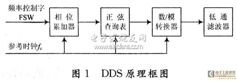
DDS technology is a phase increment technology that uses digital control signals. It has the advantages of high frequency resolution, good stability, and the flexibility to generate a variety of signals. A DDS signal generator consists of a phase accumulator, a waveform number ROM table, a D/A converter, and an analog low-pass filter LPF. The principle block diagram is shown in Figure 1. The core of DDS technology is the phase accumulator. The phase accumulator generates the address value of the read data under the control of a stable clock signal. Then, through table lookup, the address value is converted into a digital amplitude sequence of the signal waveform. The digital/analog converter (D/A) converts the digital sequence representing the waveform amplitude into an analog voltage; finally, the step-shaped waveform output by the D/A is smoothed into the desired continuous waveform through a low-pass filter. The DDS signal generator changes the output frequency by changing the value of the phase increment register △phase (the degree of each clock cycle). Whenever the output latch of the N-bit full adder receives a clock pulse, the frequency control word latched in the phase increment register is added to the output of the N-bit full adder. After the output of the phase accumulator is latched, it serves as an addressing address of the waveform memory. The content in the waveform memory corresponding to this address is the amplitude value of a waveform synthesis point, which is then converted into an analog value output through D/A conversion. When the next clock arrives, the output of the phase accumulator adds the frequency control word again, so that the address of the waveform memory is at the next amplitude point of the synthesized waveform. Finally, the phase accumulator retrieves enough points to form the entire waveform. The waveform of the synthesized signal depends on the amplitude sequence in the ROM table. Any waveform can be generated by modifying the data. If you want to generate multiple waveforms, you only need to store the required multiple waveform data in the waveform ROM table.
The frequency calculation formula of the DDS system output sine wave is:
Where: fo is the frequency of the output sine wave; fo is the system clock frequency; FSW is the frequency control word; N is the word length of the phase accumulator, and the frequency control word is proportional to the output frequency. According to the sampling theorem, the generated signal frequency can exceed 50% of the clock frequency. In practical applications, in order to ensure the output quality of the signal, the output frequency should not be higher than 33% of the clock frequency to avoid aliasing or harmonics falling into the useful output frequency band.
The frequency resolution of DDS is defined as:
Since the frequency of the reference clock is generally fixed, the number of bits of the phase accumulator determines the frequency resolution; the more bits, the higher the resolution.
The signal source uses the DDS dedicated chip AD9850 to generate a sine signal. AD9850 uses CMOS technology, and its power consumption is 155 mW when powered by 3.3 V. The extended industrial temperature range is -40 to +80 °C. It uses a 28-pin SSOP surface package. AD9850 contains a programmable DDS system and a high-speed comparator, which can realize full digital programming and control of frequency synthesis. The clock input supported by AD9850 is up to 125 MHz, and the number of bits of the frequency control word is 32 bits. From formula (2), it can be calculated that the resolution is 0.021 9 Hz when the clock input is 125 MHz. In this design, a 30 MHz active crystal oscillator is selected, so its resolution is 0.006 9 Hz calculated according to formula (2).
1.2 Overall system design
The system uses MSP430F149 to control DDS to form a square wave sine wave signal source. The system block diagram is shown in Figure 2.
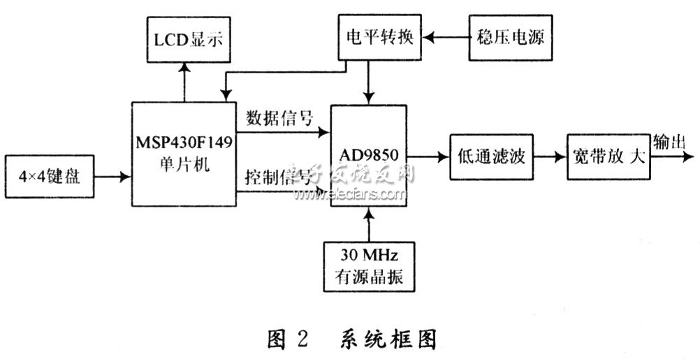
The signal source is composed of MSP430F149 single-chip microcomputer, DDS chip AD9850, low-pass filter (LPF), 4×4 soft keyboard, 1602 LCD display, external reference clock source, broadband amplifier and regulated power supply, etc. Among them, the low-pass filter is the key component in the signal source, which is responsible for filtering out high frequency, stray signals and harmonic signals in the sinusoidal output signal; the +5 V voltage of the regulated power supply provides +3.3 V power supply voltage for MSP430 and AD9850 after level conversion; the external reference clock source uses a 30 MHz active crystal oscillator, and the MSP430F149 and AD9850 are connected in serial communication.
1.3 Hardware Design
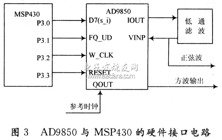
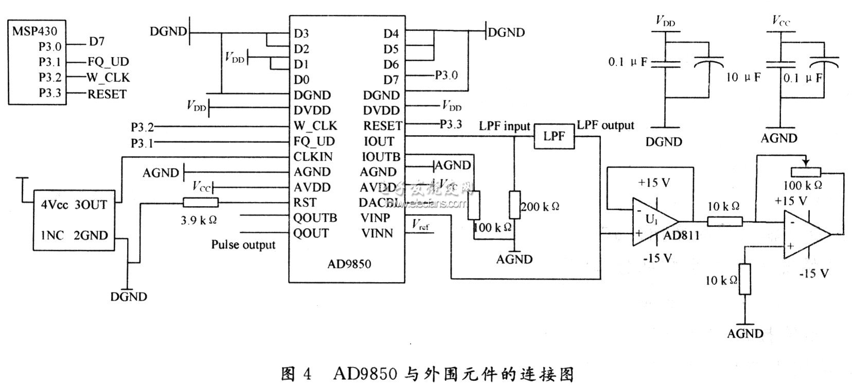
The signal source uses MSP430F149 as the core controller. In order to save I/O resources and facilitate system function expansion, serial communication is adopted between MSP430 and DDS chip AD9850. The interface circuit is shown in Figure 3. The hardware connection diagram of AD9850 and peripheral components is shown in Figure 4. The sine output signal terminal IOUT of AD9851 is connected to the external low-pass filter. After filtering out high-frequency spurious and harmonic waves, one signal is amplified by the wide amplifier AD811 and outputs the required sine signal. The other signal is then connected back to the positive input terminal (VINP) of the internal comparator of AD9851 to obtain a square wave signal. Among them: DGND is the digital ground; AGND is the analog ground; VCC is the power supply voltage of the analog part; VDD is the power supply voltage of the digital part. D7, FQ_UD, W_CLK, RESET are connected to P3.0, P3.1, P3.2, and P3.3 of MSP430 respectively. In order to reduce the impact of noise signals on the amplifier, a high-speed voltage follower is connected between the low-pass filter and the broadband amplifier for isolation. The peak-to-peak value of the output signal of AD9850 is 1-2 V. In order to increase the amplitude of the output signal of AD9850, a high-speed broadband operational amplifier AD811 with a unit gain bandwidth of 140 MHz and Sr=2 500 V/μs is used for signal amplification, and the gain is changed by adjusting the feedback resistor to adjust the output signal amplitude. The maximum amplification factor of the amplifier circuit can meet general application requirements.
1.4 Low-pass filter design
The low-pass filter is an important part of the direct digital frequency synthesizer, and its performance directly affects the characteristics of the entire direct digital synthesizer. In the entire DDS implementation process, the low-pass filter not only filters out high-frequency signals, but also has the function of removing spurious signals. The spurious signals of DDS mainly come from the following three aspects:
(1) ROM amplitude quantization error: The conversion of phase into amplitude is achieved by addressing ROM. However, the word length of the waveform amplitude value stored in the ROM address is limited. The truncation error caused by the limited ROM storage capacity is the amplitude quantization error.
(2) Phase truncation error: In order to improve the accuracy of DDS, the number of bits of the phase accumulator of DDS is very large, but the capacity of ROM is limited, so only the high M bits of the phase accumulator are used for ROM addressing, and the low (NM) bits are truncated. The truncation error introduced by this is the main source of DDS spurious;
(3) DAC conversion error, that is, the conversion error caused by nonlinearity in DAC: the limited resolution, nonlinear characteristics and spike pulses in the conversion process of DAC will lead to the deterioration of spectrum quality. Therefore, the use of low-pass filter is very necessary, and its performance is directly related to the technical indicators of the entire DDS.
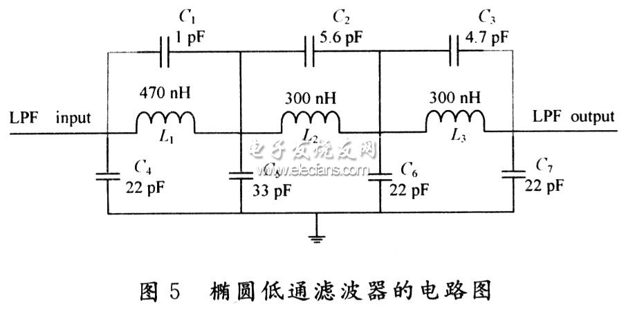
Low-pass filters can be divided into Butterworth filter, Chebyshev filter, Bessel filter and elliptic filter. The passband and stopband of Butterworth low-pass filter are flat, but its transition band is too flat; the passband of Chebyshev low-pass filter is equiripple jitter, the stopband is flat, and the transition band is slightly steeper than Butterworth; Bessel low-pass filter is just the opposite of Chebyshev low-pass, the passband is flat, and the stopband is equiripple jitter; the passband and stopband of elliptic low-pass filter are jitter. However, its transition band drops rapidly and the transition band is very narrow. In this system, in order to minimize the interference of 30 MHz of AD9850 external system clock when the output signal frequency is up to 10 MHz, an elliptic filter with a narrow transition band characteristic is used, and a 7th-order elliptic low-pass filter is used. According to system requirements, the frequency of the output signal can reach 10 MHz, and its passband is set to 10 MHz. The 7th-order filter has a faster transition band, which can effectively filter out high-frequency interference above 10 MHz. Considering that the actual elliptic filter design is different from the theoretical analysis, the specific parameters of the elliptic filter are obtained after simulation using Multisim 9. The circuit diagram of the elliptic low-pass filter is shown in Figure 5.
2 System Software Design
The software design is mainly divided into two parts: menu operation and frequency control value calculation. In the system, the set frequency and adjustment step are input through an external 4×4 soft keyboard. There are 16 keys in total, and different keys represent different numbers and functions. In addition to the normal 10 numeric keys 0 to 9, in order to facilitate the input of frequency values, function keys such as menu key, delete key, step one, step ten, confirmation key, and output key are also designed. Enter the set frequency by entering the numeric keys 0 to 9; press the confirmation key to output the waveform of the corresponding frequency; press the menu key, and press the 1, 2, and 3 numeric keys as needed to select the frequency step of 1 Hz, 10 Hz, and 100 Hz respectively; press the confirmation key, and then press step + and step one to step the frequency of the output signal; to reset the frequency, just press the delete key and enter the preset frequency again.
In this system, the microcontroller and AD9850 are connected in serial communication mode. Among them, the calculation of the frequency control word: the clock signal of AD9850 is 30 MHz, according to formula (1):
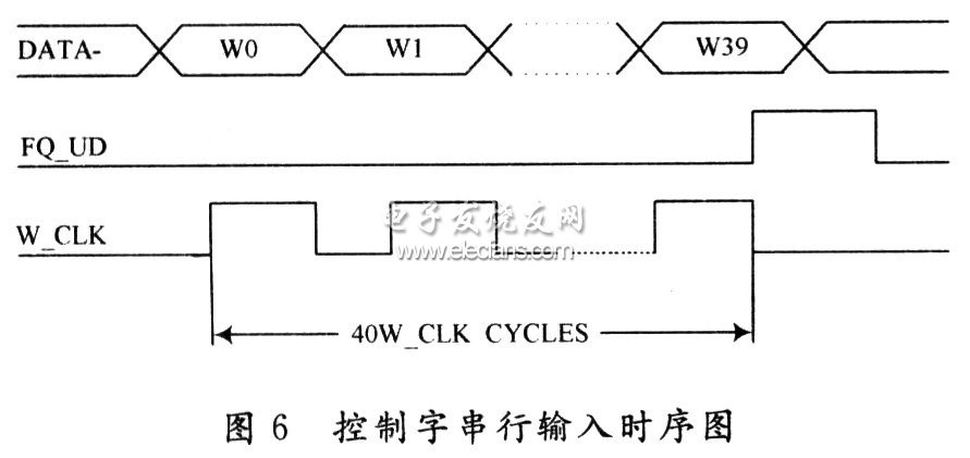
Where: fo is the frequency value entered from the keyboard. The result calculated by formula (3) is converted into a 32-bit frequency control word without affecting the accuracy by discarding the decimal part. AD9850 has a 40-bit control word, 32 bits for frequency control, 5 bits for phase control, 1 bit for power down control, and 2 bits for selecting the working mode. This 40-bit control word can be input to AD9850 in parallel or serial mode. In practical applications, the working mode selection bit is usually set to 00. In this system, the high 8 bits of the 40-bit control word of AD9850 are set to 00H. The timing relationship that needs to be met in the serial interface mode is: at the rising edge of W_CLK, the data on pin D7 is serially shifted into the input register bit by bit starting from the least significant bit. After the 40-bit data input is completed, any W_CLK rising edge will cause the data to be shifted out in sequence and the original data will be invalid. At this time, the rising edge of FQ_UD terminal loads 40 bits of data into the frequency/phase control register, updates the chip's output frequency and phase, and resets the address pointer to the first input register, waiting for the next set of new data to be written. The control word serial input timing diagram of AD9850 is shown in Figure 6.
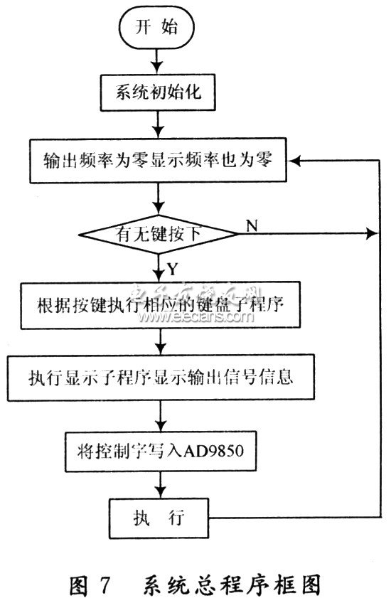
The overall program flowchart of the system is shown in Figure 7. After the program starts, the initialization program is run, including initializing the single-chip microcomputer MSP430F149 , initializing AD9850, initializing the LCD display module 1602, etc. Then scan the keyboard status, check if a key is pressed, run the key value processing program, perform table lookup processing on the key value, and then execute the corresponding subroutine. The input signal related information is displayed on the LCD by running the LCD display program. After pressing the confirmation key, the MSP430F149 calculates the data or control command of the required signal, transmits it to AD9850, and outputs the final signal.
3 System Testing and Result Analysis
In order to verify the actual performance of this system, after completing all the designs, the system was measured using an HDSTO22M oscilloscope. After experimental testing, the system achieved the following performance indicators: the output signal frequency range is 1 Hz to 10 MHz; the step adjustment is 1 Hz, 10 Hz, and 100 Hz; there is no obvious distortion; the output voltage peak-to-peak value is 1 to 10 V; and the frequency stability is better than 10-4.
4 Conclusion
Here is a design method of embedded signal source based on DDS chip AD9850 and MSP430F149 microcontroller. The signal source can output sine wave and square wave with frequency range of 1 Hz to 10 MHz, and has the function of frequency setting 1 Hz, 10 Hz, 100 Hz multi-step adjustment and amplitude adjustment. The frequency value can be set by key, and LCD displays the frequency of the waveform and other information. After experimental testing, the obtained sine wave square wave signal has the characteristics of good frequency stability, high frequency accuracy and high frequency resolution in the frequency range of 1 Hz to 10 MHz.
Previous article:Design of infrared communication interface circuit controlled by single chip microcomputer
Next article:Analysis of Ultrasonic Coded Excitation Transmission Based on DSP
- Popular Resources
- Popular amplifiers
- Molex leverages SAP solutions to drive smart supply chain collaboration
- Pickering Launches New Future-Proof PXIe Single-Slot Controller for High-Performance Test and Measurement Applications
- CGD and Qorvo to jointly revolutionize motor control solutions
- Advanced gameplay, Harting takes your PCB board connection to a new level!
- Nidec Intelligent Motion is the first to launch an electric clutch ECU for two-wheeled vehicles
- Bosch and Tsinghua University renew cooperation agreement on artificial intelligence research to jointly promote the development of artificial intelligence in the industrial field
- GigaDevice unveils new MCU products, deeply unlocking industrial application scenarios with diversified products and solutions
- Advantech: Investing in Edge AI Innovation to Drive an Intelligent Future
- CGD and QORVO will revolutionize motor control solutions
- Innolux's intelligent steer-by-wire solution makes cars smarter and safer
- 8051 MCU - Parity Check
- How to efficiently balance the sensitivity of tactile sensing interfaces
- What should I do if the servo motor shakes? What causes the servo motor to shake quickly?
- 【Brushless Motor】Analysis of three-phase BLDC motor and sharing of two popular development boards
- Midea Industrial Technology's subsidiaries Clou Electronics and Hekang New Energy jointly appeared at the Munich Battery Energy Storage Exhibition and Solar Energy Exhibition
- Guoxin Sichen | Application of ferroelectric memory PB85RS2MC in power battery management, with a capacity of 2M
- Analysis of common faults of frequency converter
- In a head-on competition with Qualcomm, what kind of cockpit products has Intel come up with?
- Dalian Rongke's all-vanadium liquid flow battery energy storage equipment industrialization project has entered the sprint stage before production
- Allegro MicroSystems Introduces Advanced Magnetic and Inductive Position Sensing Solutions at Electronica 2024
- Car key in the left hand, liveness detection radar in the right hand, UWB is imperative for cars!
- After a decade of rapid development, domestic CIS has entered the market
- Aegis Dagger Battery + Thor EM-i Super Hybrid, Geely New Energy has thrown out two "king bombs"
- A brief discussion on functional safety - fault, error, and failure
- In the smart car 2.0 cycle, these core industry chains are facing major opportunities!
- Rambus Launches Industry's First HBM 4 Controller IP: What Are the Technical Details Behind It?
- The United States and Japan are developing new batteries. CATL faces challenges? How should China's new energy battery industry respond?
- Murata launches high-precision 6-axis inertial sensor for automobiles
- Ford patents pre-charge alarm to help save costs and respond to emergencies
- Recommend several books on computer vision and image processing with OpenCV
- Sugar Glider ④ RSL10-SENSE-GEVK Playing with BHI160, step count, motion recognition? No need to process, get it directly!!
- How to solve this ESD problem
- STC12C5A60S2 MCU pattern water light (birds returning home) C program
- Goodbye 2019, hello 2020 Looking forward to the future
- 【RPi PICO】Some routines by enthusiast romilly
- Did you know? Key advantages of power management integrated circuits
- The problem of TPS55340 output voltage noise is relatively large
- Newbie wants to convert assembly language to C language
- China Huawei PCB design related specifications

 AD9850 Signal Generator Module
 ISL28433FBZ-T


 京公网安备 11010802033920号