0 Introduction
At present, many electronic devices not only require the power supply to provide two or more mutually isolated and highly regulated power supplies, but also require the power supply efficiency to be continuously improved and the power density to be continuously increased, thereby reducing the size of the circuit. The combination of these requirements puts forward higher requirements for power supply design.
Generally speaking, any topology that uses transformer isolation and can provide multiple windings on the secondary side can be a candidate for a multi-output converter. Currently, from the perspective of low cost and relatively high efficiency, multi-output circuits mostly use multi-winding output forward converters or flyback converters.
The flyback converter with multiple winding outputs is the simplest and easiest to implement among the multiple output circuits. It has many advantages, such as simple structure, low cost, and easy design. However, due to the low overall efficiency of this type of circuit, it is rarely used in applications above 150W.
The characteristics of the forward converter are exactly opposite to those of the flyback converter. The converter has the advantage of high overall efficiency and is therefore widely used in high-power applications. However, since a freewheeling diode and filter inductor are added to the secondary side of the circuit, the cost will increase accordingly [1].
In actual circuit design, the following situation may occur: the output power is not evenly distributed on each output of a multi-output power supply. That is, one or two of the outputs require a particularly large output power, accounting for more than 80% of the total output power, while the other outputs are particularly small. If the total power of the entire circuit exceeds 150W. From the perspective of efficiency, a forward converter should be used in the circuit topology. However, if a forward circuit is used for each output, the cost of several low-power circuits will be too high and unnecessary.
In view of this situation, this paper proposes a new type of multi-channel output forward-flyback converter. This converter can use the forward part of the circuit to output high power, and use the flyback part to output low power. It is a compromise between the forward converter and the flyback converter, and fully combines the high efficiency of the forward converter and the low cost of the flyback converter. Therefore, this circuit is particularly suitable for those occasions where the output power of each channel in the multi-channel output circuit is very different. At the same time, in order to enable each channel to have accurate output, the post-stage adjustment technology is also used in the output part circuit of the auxiliary circuit to accurately control the output voltage.
1 Working Principle
FIG1 shows a block diagram of the multi-channel output forward-flyback converter.

Figure 1: Multi-output forward-flyback converter using post-stage regulation technology
This circuit uses the output filter inductor in the forward converter as the flyback transformer for other auxiliary output circuits. In the time period (1-D)Ts, the energy distribution of the secondary inductor between the outputs is essentially the same as that of the flyback converter circuit (where D is the duty cycle of the main S1 and Ts is the switching period).
Like ordinary flyback converters, without other post-stage adjustment measures added to the circuit, the adjustment rate of the other auxiliary outputs without feedback in this converter will be relatively poor, usually fluctuating around 10%. If each circuit is required to have an accurate output, the most common method is to add a linear voltage regulator chip (such as 7805, etc.) to the auxiliary output. However, this will bring huge power loss, so this method is only applicable to low output power occasions. In medium and high power occasions, the commonly used method is magnetic switch (magamp). However, in high frequency occasions, post-stage adjustment technology (SSPR) has more advantages [2]. Therefore, this article uses this technology to obtain accurate output voltage on other auxiliary output windings.
For the flyback converter, when the main circuit is turned off, the energy is transferred from the primary inductor to the load side in the form of a current source. More importantly, there is no output inductor in the flyback converter, and the output voltage of each circuit is determined by the turns ratio of the transformer. That is, the main circuit output voltage and the auxiliary circuit output voltage in the flyback circuit are determined by formula (1).
Uo1/N1=Uo2/N2(1)
In this working mode, if the circuit is not adjusted, the voltage blocking characteristic of SSPR will not work at this point. Therefore, a "time-division multiplexing" mode is proposed in the literature [3]. In this mode, when the main tube is turned off, energy will be transmitted to different output branches in different time periods. In order to achieve the "time-division multiplexing" working state, equation (2) must be satisfied.
Uo1/N1>Uo2/N2 (2)
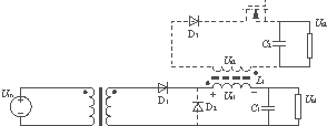
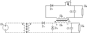
Figure 2 shows several main working waveforms of the circuit. Figure 3 shows the equivalent circuit diagram of each stage of the converter using SSPR. (ugs1 is the gate signal of the main switch S1. ugs2 is the gate signal of the auxiliary switch S2)
(a) Phase 1 DTs

(b) Stage 2 D1Ts
(c) Stage 3 D2Ts
Figure 3 Equivalent circuit diagram of each stage
The specific working process is described as follows.
The main output Uo1 of the circuit controls the opening time of the main tube through feedback-controlled PWM, thereby determining the amount of energy transmitted to the secondary side of the transformer. The role of SSPR is to transmit this energy to different output branches in the (1-D)Ts time period, so as to achieve the purpose of distributing this part of energy between the two outputs Uo1 and Uo2. "Time-division multiplexing" can be achieved by adjusting the blocking time of SSPR.
Phase 1 Before time t1, in the time period DTs, as shown in Figure 3(a), the main switch S1 is turned on, and part of the energy on the DC bus is stored in the output inductor L1 through the forward transformer, and the other part is transferred to the main output Uo1.
UL1=Us1=Uin/n-Uo1(3)
Where: n is the transformation ratio of the forward transformer T.
Phase 2 After t1, in the time period D1Ts (D1 is the duty cycle of diode D2), as shown in Figure 3(b), the main S1 and diode D1 are turned off, and the SSPR blocks the auxiliary output. Therefore, at this time, only the diode D2 on the Uo1 branch is turned on. The voltage Us1 on the inductor L1 is clamped on the main output voltage Uo1.
UL1=-Us1=-Uo1(4)
Phase 3 In the time period D2Ts (D2 is the duty cycle of S2), as shown in Figure 3(c), S2 on the secondary side of the transformer has been triggered to turn on, and D3 is also turned on. From equation (2), it can be seen that the voltage Us1 on L1 will be clamped at N1Uo2/N2
UL1=-Us1=-N1Uo2/N2(5)
In summary, the output inductor L1 of the forward converter not only transfers energy to Uo1 in phase 2, but also acts as a flyback transformer to transfer energy to Uo2 in the D2Ts period. In a period of time, only one output branch obtains energy.
The time period D2Ts can be realized by the feedback control circuit of SSPR, while the time period DTs is realized by the PWM control of the forward circuit. Since D+D1+D2=1, D1Ts=(1-D-D2)Ts, then D1Ts will be determined by DTs and D2Ts. Therefore, this circuit will be able to obtain two precise output circuits Uo1 and Uo2.
Assuming that the current on the forward output inductor L1 is continuous, we can analyze the volt-second balance of L1 and get
(Uin/n-Uo1)DTs=Uo1D1Ts+(N1Uo2/N2)D2Ts(6)
In order to simplify formula (6), it is assumed that
ΔU=Uo1-N1Uo2/N2(7)
but
Uo1=(Uin/n-ΔU)D+ΔU(8)
D =
![]() (9)
(9)
2 Experimental Results
A 250W prototype with 2 outputs verifies the working principle and advantages of the converter.
The specifications and main parameters of the converter are as follows:
Input voltage Uin 220 (1 ± 20%) V;
Main output voltage Uo1 24V;
Main output current Io 11~10A;
Auxiliary circuit output voltage Uo2 12V;
Auxiliary circuit output current Io2 0~1A;
Output powerPo 250W;
Working frequency f 100kHz;
Main switch S1 IRFP840;
Rectifier diodes D1, D2 MBR20200CT;
Rectifier diode D3 8TQ100;
The turns ratio of the primary and secondary sides of the transformer TPQ3230 is 32:8;
The original secondary turns ratio of inductor L1 is 40:25, and the magnetic core is A-548127-2 from ARNOLD;
The control chip of SSPR is UCC3583 from TI.
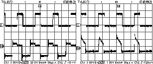
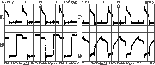
Figure 4 shows several key waveforms of the converter. These waveforms show that when the gate signal ugs2 is high, S2 is turned on, and the voltage uDS1 changes from the previous output voltage Uo1 to the voltage N1Uo2/N2
(a) ugs2 and uDS1 of S2 (b) ugs2 and iD2
(c)iD2 and uDS1 (d)iD2 and iD1
Figure 4 Experimental waveform
FIG5 shows the efficiency curve of the converter at different Po, with the highest reaching 92.4% and the maximum reaching 89.36% at full load.
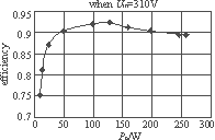
Figure 5 Efficiency curves at different output powers
Figure 6 shows the load regulation curve of the converter before and after the application of SSPR, which fully demonstrates that after the application of SSPR, the auxiliary output has a good regulation rate for all output states.
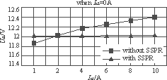
(a) When the auxiliary output is unloaded
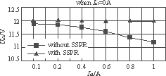
(b) When the main output is in no-load state
Figure 6 Load regulation of auxiliary output UO2
3 Conclusion
This paper proposes a novel multi-output forward-flyback converter using post-stage regulation technology (SSPR). It combines the advantages of high efficiency of the forward converter and low cost of the flyback converter, while ensuring accurate output of each voltage. This circuit is particularly suitable for applications where the output power of each channel is very unbalanced and high efficiency and accurate output are required. A 250W prototype verifies its advantages.
Previous article:Design of capacitive touch button based on charging and discharging principle
Next article:Comparison between hysteresis modulation and unipolar frequency multiplication modulation for 6kV·A inverter
Recommended ReadingLatest update time:2024-11-16 23:41


- Popular Resources
- Popular amplifiers
-
 西门子S7-12001500 PLC SCL语言编程从入门到精通 (北岛李工)
 -
 New Energy Vehicle Detection and Diagnosis Experiment (Edited by Mao Caiyun, Zhou Xien, and Long Jiwen)
 -
 Virtualization Technology Practice Guide - High-efficiency and low-cost solutions for small and medium-sized enterprises (Wang Chunhai)
 -
 ESP32-S3 source code
- MathWorks and NXP Collaborate to Launch Model-Based Design Toolbox for Battery Management Systems
- STMicroelectronics' advanced galvanically isolated gate driver STGAP3S provides flexible protection for IGBTs and SiC MOSFETs
- New diaphragm-free solid-state lithium battery technology is launched: the distance between the positive and negative electrodes is less than 0.000001 meters
- [“Source” Observe the Autumn Series] Application and testing of the next generation of semiconductor gallium oxide device photodetectors
- 采用自主设计封装,绝缘电阻显著提高!ROHM开发出更高电压xEV系统的SiC肖特基势垒二极管
- Will GaN replace SiC? PI's disruptive 1700V InnoMux2 is here to demonstrate
- From Isolation to the Third and a Half Generation: Understanding Naxinwei's Gate Driver IC in One Article
- The appeal of 48 V technology: importance, benefits and key factors in system-level applications
- Important breakthrough in recycling of used lithium-ion batteries
- Innolux's intelligent steer-by-wire solution makes cars smarter and safer
- 8051 MCU - Parity Check
- How to efficiently balance the sensitivity of tactile sensing interfaces
- What should I do if the servo motor shakes? What causes the servo motor to shake quickly?
- 【Brushless Motor】Analysis of three-phase BLDC motor and sharing of two popular development boards
- Midea Industrial Technology's subsidiaries Clou Electronics and Hekang New Energy jointly appeared at the Munich Battery Energy Storage Exhibition and Solar Energy Exhibition
- Guoxin Sichen | Application of ferroelectric memory PB85RS2MC in power battery management, with a capacity of 2M
- Analysis of common faults of frequency converter
- In a head-on competition with Qualcomm, what kind of cockpit products has Intel come up with?
- Dalian Rongke's all-vanadium liquid flow battery energy storage equipment industrialization project has entered the sprint stage before production
- Allegro MicroSystems Introduces Advanced Magnetic and Inductive Position Sensing Solutions at Electronica 2024
- Car key in the left hand, liveness detection radar in the right hand, UWB is imperative for cars!
- After a decade of rapid development, domestic CIS has entered the market
- Aegis Dagger Battery + Thor EM-i Super Hybrid, Geely New Energy has thrown out two "king bombs"
- A brief discussion on functional safety - fault, error, and failure
- In the smart car 2.0 cycle, these core industry chains are facing major opportunities!
- The United States and Japan are developing new batteries. CATL faces challenges? How should China's new energy battery industry respond?
- Murata launches high-precision 6-axis inertial sensor for automobiles
- Ford patents pre-charge alarm to help save costs and respond to emergencies
- New real-time microcontroller system from Texas Instruments enables smarter processing in automotive and industrial applications
- Operational amplifier stability analysis problem
- 【NXP Rapid IoT Review】+ My Review Summary
- VHDL Introduction. Questions and Answers. Classic Examples. Experience Summary
- ROM and RAM How does the microcontroller execute step by step after power is turned on?
- How does the program execute from the reset sequence to the main function?
- [AutoChips AC7801x motor demo board review] + Motor drive - BLDC sensorless method
- EEWORLD University ---- Practical Projects for IoT Embedded Engineers
- AC 220v to DC 24v (LM7824CT)
- Today's live broadcast! How to design high-performance servo drives using Infineon IGBT7
- STM32MP157A-DK1 Evaluation + HelloWorld and GPIO (2)

 西门子S7-12001500 PLC SCL语言编程从入门到精通 (北岛李工)
 ESP32-S3 source code


 京公网安备 11010802033920号