summary:
This paper introduces the impact and evaluation of cosmic radiation on the reliability of high-voltage power semiconductor devices in automotive OBC and high-voltage to voltage DCDC applications.
Keywords: OBC; DCDC; cosmic radiation; FIT
introduction:
The automotive industry is developing rapidly and innovating, so the application of on-board chargers (OBC) and DCDC converters (HV-LV DC-DC) has also developed rapidly. Like most engineering challenges, designers have turned their attention to advanced technologies, hoping to use modern Super Junction Si technology and Silicon Carbide (SiC) technology to provide solutions. While pursuing performance, reliability is also an important topic for automotive products.
In automotive OBC/DCDC applications, high-voltage power semiconductor devices are increasingly used. For automotive-grade high-voltage semiconductor power devices, gate oxide robustness and cosmic radiation robustness are two very important aspects of reliability.
Cosmic radiation is rarely mentioned, but the fact is that high-voltage power semiconductor devices of any technology will be affected by radiation and cause transient failures of a few nanoseconds, and it is difficult to locate the cause of cosmic radiation. Many power semiconductor applications require a single device failure rate of 1-100 FIT or even lower, so in high-voltage automotive applications, the impact of cosmic radiation needs to be recognized and taken seriously.
Therefore, this paper will focus on the application of bidirectional OBC/DCDC, explain the impact of cosmic radiation and the method of evaluating system reliability.
1. Mechanism of the impact of cosmic radiation on reliability
1. Main factors of automotive-grade high-voltage device reliability
The FIT rate of automotive-grade high-voltage (above 650V) devices is mainly affected by the robustness of the gate oxide layer and the robustness of cosmic radiation. The processing of the gate oxide layer is different for SiC devices and Si devices due to differences in material hardness, band gap, trap density, etc. Despite this, Infineon has made a lot of efforts and research in SiC, so that the robustness of the gate oxide layer has reached a very high level.
In both SiC and Si, the failure rate due to cosmic radiation increases exponentially with the electric field present in the device at the time of incidence. Devices with similar electric fields have similar failure rates. Many accelerated tests have been performed over the past few decades, which have shown that the failure rates induced by cosmic rays are similar when the applied voltage is normalized to the actual avalanche breakdown voltage. There are only relatively subtle differences between Si and SiC technology in terms of the basic failure mechanisms caused by cosmic rays and their relationship to operating conditions. In general, vertical power devices can be designed with higher avalanche breakdown voltages, which allows for greater cosmic radiation resistance through greater thickness and lower doping of the drift or substrate layers.

Figure 1: Main factors of FIT rate
2. What is cosmic radiation?
The life of a certain number of devices is usually described by a bathtub curve. It is divided into early failure period, accidental failure period and wearout failure period. Early failure period can be screened by early testing. For well-designed devices, wearout failure period only occurs in the time period outside the specification. Accidental failure period is the main consideration for failure during the product life cycle. The failure effect of cosmic radiation on high-voltage power devices belongs to this category.
Single event burnouts (SEBs) caused by cosmic radiation are a factor in the occasional failure of high-voltage MOSFETs. Although failure is accidental, the failure rate can be predicted and evaluated by understanding the application conditions. This article will introduce the single event burnout time and the basic method for predicting the failure rate of high-voltage MOSFETs caused by cosmic radiation.

Figure 2: Bathtub Curve
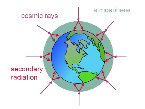
Cosmic radiation bombards the Earth with high-energy particles, mainly protons and heavy nuclei. In a few cases, the energy of the particles measured is as high as 10 20 eV. Due to the existence of the atmosphere, these particles collide with the nuclei of atoms in the outer atmosphere, producing secondary particles, which carry the energy of the primary particles.
Generally speaking, these secondary particles have enough energy to produce more particles in subsequent collisions, resulting in avalanche multiplication. But at the same time, the density of particles will be reduced due to absorption by the atmosphere. As shown in the figure below:

Figure 3: Generation of secondary particles
3. Effects of cosmic radiation on power semiconductors
When the secondary particles reach the surface of the earth, they interact with dense matter. For high-voltage MOSFETs, this means that there is a certain probability of being bombarded in the blocking area. Particles usually bombard the device with an energy of several hundred MeV (100MeV≈16pJ), generating electron-hole pairs within a few millimeters. From the analysis of energy spectrum components, neutrons are the only type of particles that are numerous and can concentrate energy to one point and produce burns, which are called single-element burns (SEBs). Therefore, neutrons are the most harmful component.
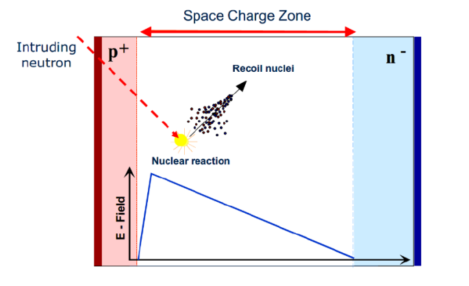
A brief explanation of the failure mechanism of single event burnout (SEBs): Figure 4 (1) shows the electric field distribution of the pn junction in the reverse bias state before the neutron penetrates:

Figure 4 (1): Electric field distribution at the moment of no penetration
When neutrons collide with Si/SiC nuclei of MOSFETs, recoil ions are generated. The kinetic energy of the ions triggers a small-scale charge explosion within a few millimeters. In the off state, these charge-carrying plasmas shield their interior from the electric field. At the edge of the plasma zone, high peak electric field strengths are established. During the ionization process generated by the corresponding collisions, the peak electric field gradually expands, thereby extending the range of the ion zone.
This self-sustaining process is called "streamer". The expansion of the plasma zone will eventually cause the Drain and Source to be electrically short-circuited. The heat generated by the short-circuit will melt the Si and eventually destroy the MOSFETs structure, causing it to fail.

Figure 4 (2): Electric field distribution after invasion
Since the failure mechanism is caused by the impact ionization process, it does not occur in the MOSFETs conduction mode, that is, in the absence of high-intensity electric fields, so the conduction mode does not need to be considered when evaluating the failure rate.
2. FIT rate
-
definition
The FIT (failures in time) value of a device refers to the number of failed devices when 1 billion devices are running for a certain period of time. For example, 1 FIT/device. The formula is as follows:

N: total number of tested devices
F: Total number of failed devices
T: total test hours
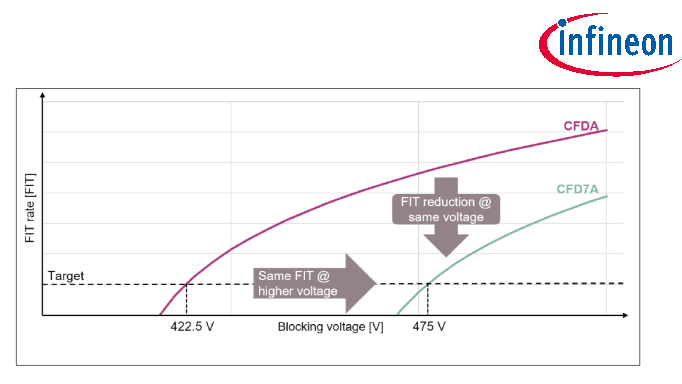
Figure 5 is a schematic diagram of the relationship between the FIT rate and voltage of two generations of automotive-grade CoolMOS for easier understanding:

Figure 5: Comparison of FIT rates between two generations of automotive grade
2. Influencing factors
The FIT rate curve is usually defined under the conditions of 25°C and 0 altitude per unit area. From the definition, it can be seen that FIT is related to the following conditions:
Turn-off voltage: As mentioned above, the cosmic radiation failure mechanism occurs under the turn-off condition, so the turn-off voltage has a great relationship with the failure rate, which can also be seen from Figure 5.
Altitude: The higher the ion density at high altitude, the exponential relationship between sea wave and failure rate. The FIT at 3000 meters is an order of magnitude higher than that at sea level.
Junction temperature: Temperature and failure rate have an inverse characteristic. The higher the temperature, the lower the failure rate. The failure rate at 125°C is one order of magnitude lower than that at 25°C.
Chip area: The failure rate is linearly related to the chip area. The larger the area, the greater the probability of neutron bombardment.
On/off state: FIT is linearly related to the off time
3. How to measure radiation failure rate
Measurements in natural radiation environments
The simplest way is the storage test, where a certain number of devices are radiated and measured at a given bias voltage until failure occurs, and the combination of tests is performed under different variables, such as Vds and temperature.
This test method is only applicable to failure rates near the limit voltage. It is not applicable to conditions where the actual working voltage has a large deviation from V(BR)DSS. For this situation, accelerated testing is required at a relatively low voltage, which requires artificial radiation sources to accelerate, in order to avoid a long time of several years or a large number of samples.
Accelerated testing
At high altitudes, the radiation density increases, so testing in high altitude areas can be considered an accelerated test. The advantage of this method is that it can reflect the actual radiation status. For example, some institutions will test at the Zugspitze test point in Germany at an altitude of 2,962 meters. The disadvantage of this method is that it is relatively difficult to access and the acceleration factor rarely exceeds 10.
Previous article:EMC filter design with REDEXPERT
Next article:WPG Group launches 100W PD power adapter solution based on Onsemi products
Recommended ReadingLatest update time:2024-11-16 20:48

- MathWorks and NXP Collaborate to Launch Model-Based Design Toolbox for Battery Management Systems
- STMicroelectronics' advanced galvanically isolated gate driver STGAP3S provides flexible protection for IGBTs and SiC MOSFETs
- New diaphragm-free solid-state lithium battery technology is launched: the distance between the positive and negative electrodes is less than 0.000001 meters
- [“Source” Observe the Autumn Series] Application and testing of the next generation of semiconductor gallium oxide device photodetectors
- 采用自主设计封装,绝缘电阻显著提高!ROHM开发出更高电压xEV系统的SiC肖特基势垒二极管
- Will GaN replace SiC? PI's disruptive 1700V InnoMux2 is here to demonstrate
- From Isolation to the Third and a Half Generation: Understanding Naxinwei's Gate Driver IC in One Article
- The appeal of 48 V technology: importance, benefits and key factors in system-level applications
- Important breakthrough in recycling of used lithium-ion batteries
- Innolux's intelligent steer-by-wire solution makes cars smarter and safer
- 8051 MCU - Parity Check
- How to efficiently balance the sensitivity of tactile sensing interfaces
- What should I do if the servo motor shakes? What causes the servo motor to shake quickly?
- 【Brushless Motor】Analysis of three-phase BLDC motor and sharing of two popular development boards
- Midea Industrial Technology's subsidiaries Clou Electronics and Hekang New Energy jointly appeared at the Munich Battery Energy Storage Exhibition and Solar Energy Exhibition
- Guoxin Sichen | Application of ferroelectric memory PB85RS2MC in power battery management, with a capacity of 2M
- Analysis of common faults of frequency converter
- In a head-on competition with Qualcomm, what kind of cockpit products has Intel come up with?
- Dalian Rongke's all-vanadium liquid flow battery energy storage equipment industrialization project has entered the sprint stage before production
- Allegro MicroSystems Introduces Advanced Magnetic and Inductive Position Sensing Solutions at Electronica 2024
- Car key in the left hand, liveness detection radar in the right hand, UWB is imperative for cars!
- After a decade of rapid development, domestic CIS has entered the market
- Aegis Dagger Battery + Thor EM-i Super Hybrid, Geely New Energy has thrown out two "king bombs"
- A brief discussion on functional safety - fault, error, and failure
- In the smart car 2.0 cycle, these core industry chains are facing major opportunities!
- The United States and Japan are developing new batteries. CATL faces challenges? How should China's new energy battery industry respond?
- Murata launches high-precision 6-axis inertial sensor for automobiles
- Ford patents pre-charge alarm to help save costs and respond to emergencies
- New real-time microcontroller system from Texas Instruments enables smarter processing in automotive and industrial applications
- Solution to the failure of IAR programming MSP430
- MicroPython sets up a separate factory reset code file
- Use ustruct to reorganize byte values, Pandora development board gyroscope
- Display community logo on three-color E-Ink Gizmo
- 【GD32450I-EVAL】UART
- Simple VGA driver for MicroPython
- How to solve CAN bus test problems
- Fudan Micro FM33LG0xx Series Data Summary
- How to use a computer
- [DIY] Transform electric car lights into 5V mobile power supply


 Building real-time machine learning systems
 Vehicle-mounted DCDC power supply EMC test specification V1.0


 京公网安备 11010802033920号