This article will focus on stable current sources using bipolar junction transistors (BJTs) and NMOS transistors.
Stable current source (BJT)
Target
The purpose of this experiment is to investigate how the zero gain concept can be used to produce a stable (less sensitive to changes in input current level) output current.
Material
► ADALM2000 active learning module
►Solderless Breadboard
► One 2.2 kΩ resistor (or other similar value)
► One 100 Ω resistor
► One 4.7 kΩ resistor
► Two small signal NPN transistors (2N3904 or SSM2212)
illustrate
The circuit corresponding to the BJT stable current source is shown in Figure 1.
Hardware Setup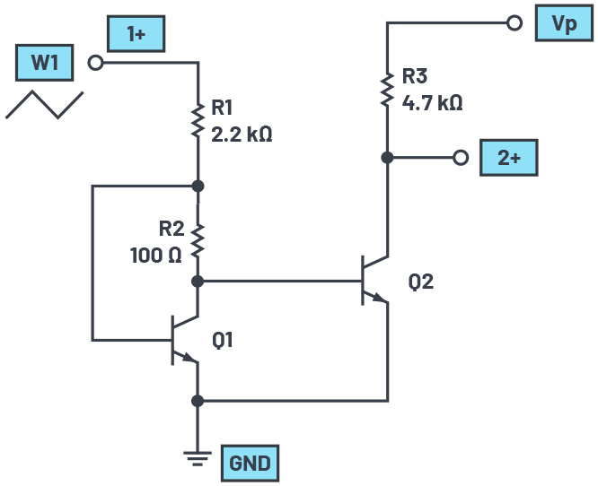
Figure 1. Steady current source
Hardware Setup
The breadboard connections are shown in Figure 2. The output of W1 drives one end of resistor R1. Resistors R1 and R2 and transistor Q1 are connected as shown in the November 2020 StudentZone article. Since Q2's VBE is always less than Q1's VBE, Q1 and Q2 are selected from stock parts where possible so that Q2's VBE is less than Q1's VBE at the same collector current. The base of transistor Q2 is connected to the zero-gain output of Q1's collector. R3 is connected between the Vp supply and Q2's collector and is used with the 2+ oscilloscope input to measure the collector current.
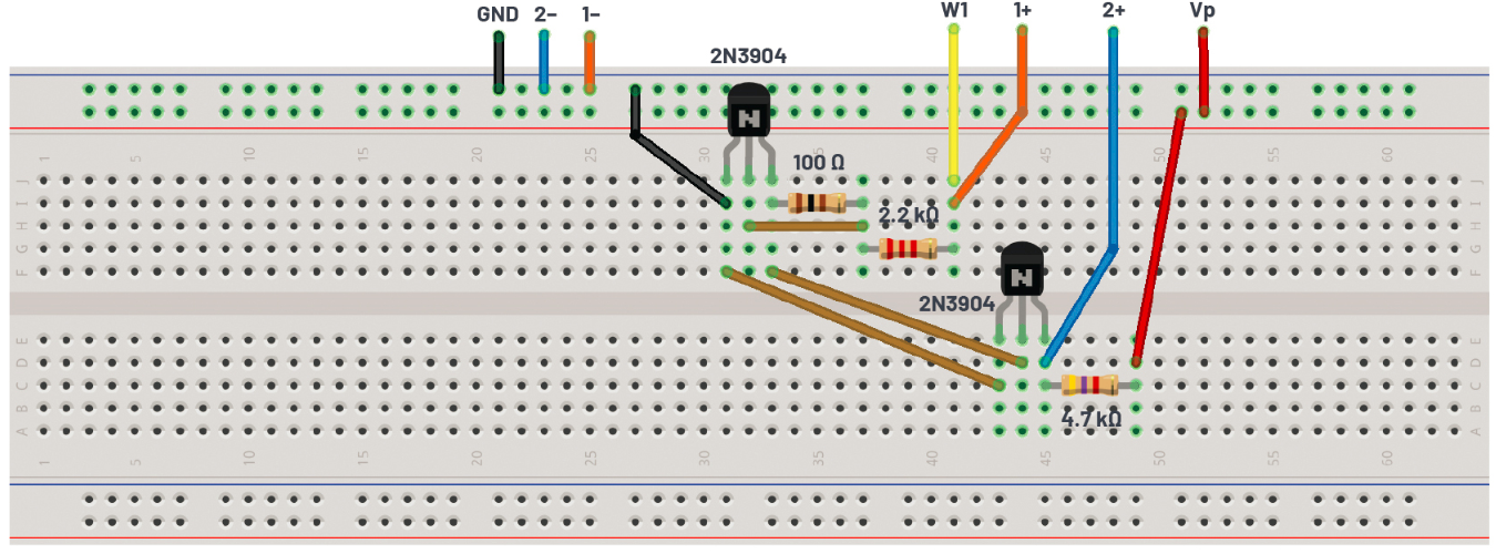
Figure 2. NMOS zero-gain amplifier breadboard circuit
Procedure
A zero-gain amplifier can be used to create a stable current source. Now, as the input supply voltage represented by W1 varies, the voltage seen by the collector of transistor Q1 is more stable, so it can be used as the base voltage of Q2 to produce a more stable current in transistor Q2.
The waveform generator is configured for a 1 kHz triangle wave with a peak-to-peak amplitude of 3 V and an offset of 1.5 V. The input (2+) of oscilloscope Channel 2 is used to measure the regulated output current at the collector of Q2.
Configure the oscilloscope to capture multiple cycles of the two signals being measured. Make sure the XY function is enabled.
Examples of waveform diagrams using an oscilloscope are shown in Figures 3 and 4.
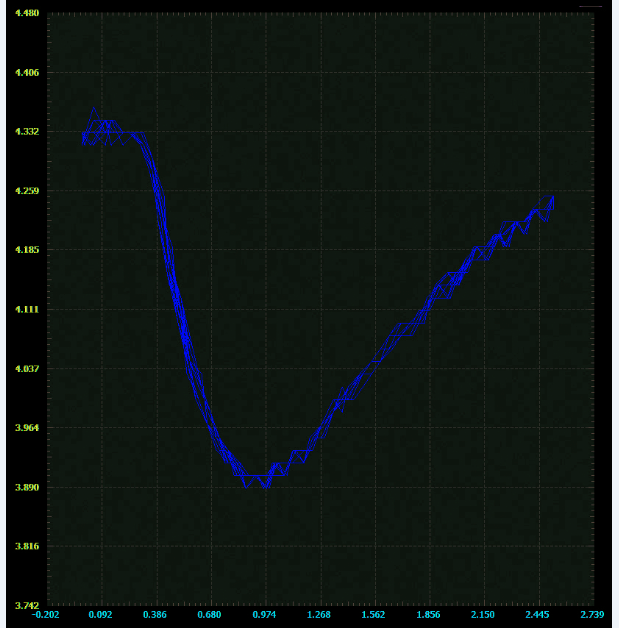
Figure 3. Relationship between Q2 collector voltage and W1 voltage
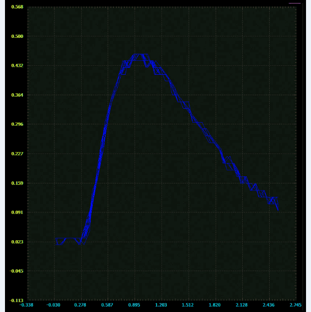
Figure 4. Oscilloscope plot of Q2 collector current vs. W1 voltage
Stable current source (NMOS)
Material
► ADALM2000 active learning module
►Solderless Breadboard
► One 2.2 kΩ resistor (or other similar value)
► One 168 Ω resistor (100 Ω and 68 Ω resistors in series)
► One 4.7 kΩ resistor
► Two small signal NMOS transistors (CD4007 or ZVN2110A)
illustrate
The circuit corresponding to the MOS stable current source is shown in Figure 5.
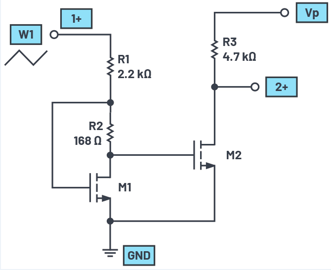
Figure 5. Stable current source
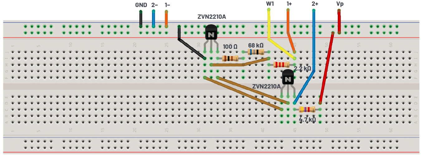
Figure 6. Steady current source breadboard circuit
Hardware Setup
The breadboard connections are shown in Figure 6. The output of waveform generator W1 drives one end of resistor R1. Resistors R1 and R2 and transistor M1 are connected as shown in the November 2020 StudentZone article. Since the VGS of M2 is always less than the VGS of M1, if possible, M1 and M2 are selected from component inventory so that the VGS of M2 is less than the VGS of M1 at the same drain current. The gate of transistor M2 is connected to the zero-gain output of the drain of M1. R3 is connected between the Vp supply and the drain of M2 and is used with the 2+ oscilloscope input to measure the drain current.
Procedure
The waveform generator is configured for a 1 kHz triangle wave with a peak-to-peak amplitude of 4 V and an offset of 2 V. The input (2+) of oscilloscope Channel 2 is used to measure the regulated output current at the drain of M2.
Configure the oscilloscope to capture multiple cycles of the two signals being measured. Make sure the XY function is enabled.
Figure 7 provides an example of an image of an oscilloscope display.
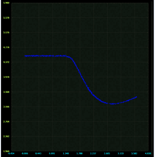
Figure 7. Relationship between M2 drain voltage and W1 voltage
Questions about BJT and NMOS
►This type of circuit is sometimes called a peaking current source. Why do you think this naming convention is used?
►The peak value of the output current is very narrow. How can I adjust the circuit to produce a wider, flatter peak?
You can find the answers to your questions on the StudentZone blog.
About the Author
Doug Mercer graduated from Rensselaer Polytechnic Institute (RPI) in 1977 with a bachelor’s degree in electrical engineering. Since joining Analog Devices in 1977, he has contributed directly or indirectly to more than 30 data converter products and holds 13 patents. He was named an ADI Fellow in 1995. In 2009, he transitioned from full-time employment and continues to serve as a consultant to ADI as a Fellow Emeritus, contributing to the Active Learning Program. In 2016, he was named Engineer-in-Residence for the ECSE Department at RPI. He can be reached at doug.mercer@analog.com.
Antoniu Miclaus is a system applications engineer at Analog Devices, working on ADI educational projects and developing embedded software for Circuits from the Lab®, QA automation, and process management. He joined Analog Devices in February 2017 in Cluj-Napoca, Romania. He is currently an MSc student in the Master of Software Engineering program at Bebis Bolyai University and holds a B.A. in Electronics and Telecommunications Engineering from the Technical University of Cluj-Napoca. He can be reached at antoniu.miclaus@analog.com.
Previous article:Microchip releases high-precision voltage reference IC for automotive applications with extremely low drift
Next article:Add flexible current limiting function
Recommended ReadingLatest update time:2024-11-16 08:25

- MathWorks and NXP Collaborate to Launch Model-Based Design Toolbox for Battery Management Systems
- STMicroelectronics' advanced galvanically isolated gate driver STGAP3S provides flexible protection for IGBTs and SiC MOSFETs
- New diaphragm-free solid-state lithium battery technology is launched: the distance between the positive and negative electrodes is less than 0.000001 meters
- [“Source” Observe the Autumn Series] Application and testing of the next generation of semiconductor gallium oxide device photodetectors
- 采用自主设计封装,绝缘电阻显著提高!ROHM开发出更高电压xEV系统的SiC肖特基势垒二极管
- Will GaN replace SiC? PI's disruptive 1700V InnoMux2 is here to demonstrate
- From Isolation to the Third and a Half Generation: Understanding Naxinwei's Gate Driver IC in One Article
- The appeal of 48 V technology: importance, benefits and key factors in system-level applications
- Important breakthrough in recycling of used lithium-ion batteries
- Innolux's intelligent steer-by-wire solution makes cars smarter and safer
- 8051 MCU - Parity Check
- How to efficiently balance the sensitivity of tactile sensing interfaces
- What should I do if the servo motor shakes? What causes the servo motor to shake quickly?
- 【Brushless Motor】Analysis of three-phase BLDC motor and sharing of two popular development boards
- Midea Industrial Technology's subsidiaries Clou Electronics and Hekang New Energy jointly appeared at the Munich Battery Energy Storage Exhibition and Solar Energy Exhibition
- Guoxin Sichen | Application of ferroelectric memory PB85RS2MC in power battery management, with a capacity of 2M
- Analysis of common faults of frequency converter
- In a head-on competition with Qualcomm, what kind of cockpit products has Intel come up with?
- Dalian Rongke's all-vanadium liquid flow battery energy storage equipment industrialization project has entered the sprint stage before production
- Allegro MicroSystems Introduces Advanced Magnetic and Inductive Position Sensing Solutions at Electronica 2024
- Car key in the left hand, liveness detection radar in the right hand, UWB is imperative for cars!
- After a decade of rapid development, domestic CIS has entered the market
- Aegis Dagger Battery + Thor EM-i Super Hybrid, Geely New Energy has thrown out two "king bombs"
- A brief discussion on functional safety - fault, error, and failure
- In the smart car 2.0 cycle, these core industry chains are facing major opportunities!
- The United States and Japan are developing new batteries. CATL faces challenges? How should China's new energy battery industry respond?
- Murata launches high-precision 6-axis inertial sensor for automobiles
- Ford patents pre-charge alarm to help save costs and respond to emergencies
- New real-time microcontroller system from Texas Instruments enables smarter processing in automotive and industrial applications
- How KiCAD schematics and PCB interact
- About Power
- Usage of $test$plusargs
- Amplifier Expert Design Experience
- Flathead RVB2601 board-web playback
- [Modification] Both the boost board and the purifier are troublesome in voltage
- Where does the magnetic flux go in this case and what is its impact?
- EEWORLD University ---- ROS Courses
- TTI&TE Live: The development and latest applications of sensors in industrial motors
- TI 28335 and AD7606 communicate via SPI serial data

 New concept analog circuit 1-5
 \"New Concept Analog Circuit\" - Transistor [Text Version] (Yang Jianguo)


 京公网安备 11010802033920号