By Selcuk Ilke
Introduction
The HMC1118 is a silicon single-pole double-throw (SPDT) switch rated for operation from 9 kHz to 13 GHz in a 4 mm × 4 mm, 16-lead leadframe chip scale package (LFCSP). This broadband switch is ideal for test and measurement equipment and high-performance wireless applications. Key features include:
• Low insertion loss: 0.68 dB (at 8 GHz)
• High isolation: 48 dB (at 8 GHz)
• High input P1 dB: 37 dBm
• High input IP3: 62 dBm
• Fast settling time (to within 0.05 dB of final RF output): 7.5 μs
The HMC1118 functional block diagram is shown in Figure 1. The HMC1118 nominally requires dual supply voltages, VDD = +3.3 V and VSS = −2.5 V, and the device is characterized at these voltages. Refer to the HMC1118 data sheet and this application note for complete characterization when operating from dual supplies.
The HMC1118 can also be powered from a single positive supply of VDD = 3.3 V, with the VSS pin tied to ground. Large signal performance is compromised with a single supply, but the device still provides very good performance for many applications where no negative supply voltage is available. This application note focuses on the operation of the HMC1118 and compares the performance of the device with single and dual supplies.
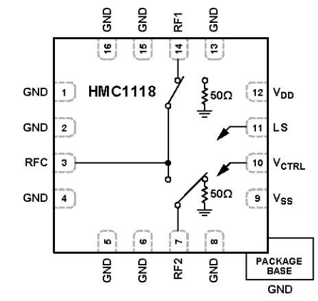
Figure 1. HMC1118 Functional Block Diagram
HMC1118 Switch Operation
The HMC1118 uses the familiar absorptive SPDT switch topology with a series field effect transistor (FET) and a shunt FET on two identical RF paths, with an integrated driver for the internal logic function, as shown in Figure 2.
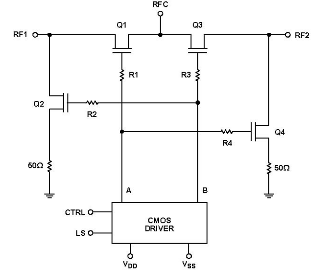
Figure 2. Simplified HMC1118 circuit diagram The
HMC1118 provides two operating modes for its RF core, as shown in Table 1. In Mode 1, the RF1 to RFC path is in the on state and the RF2 to RFC is in the isolated state; in Mode 2, the opposite is true.
In the insertion loss path, the series FET is turned on and the shunt FET is turned off. In the isolation path, the opposite is true, the series FET is turned off and the shunt FET is turned on. Therefore, the series and shunt FETs on each RF path require complementary control voltages. The HMC1118 integrates a driver on the chip to generate the A and B complementary control voltages, as shown in Figure 2. Therefore, the switch can be controlled by a single CMOS logic voltage applied to the VCTRL pin, and the LS pin can be grounded or connected to VDD (see Table 2).
Table 1. Switching Modes 
Table 2. Control Voltages 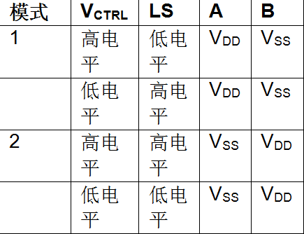
The switching FET acts as a three-port voltage-controlled device, and the RF signal conduction channel between the drain port and the source port is closed (on state) or closed (off state) according to the control voltage applied to the gate port. The HMC1118 uses N-channel enhancement mode FETs with a typical pinch-off voltage of 0.3 V, which is the potential difference between the gate and the drain-source channel required to turn on the FET. The drain and source ports of each FET are at DC ground potential, so no DC blocking capacitors are required on the RF port (which would limit low-frequency operation). Therefore, an absolute gate voltage greater than (or less than) 0.3 V turns the FET on (or off).
FETs are generally biased to extreme voltages of +3.3 V and −2.5 V to establish a certain voltage to turn the FET on and off and provide optimal RF performance. Since the HMC1118 does not have an integrated regulator and negative voltage generator, two regulated external supply voltages need to be applied to the VDD and VSS pins to generate the necessary bias voltages for the FET devices. Although the typical values of VDD and VSS are +3.3 V and −2.5 V, respectively, the user has the flexibility to operate the device with only a single positive supply, VDD = 3.3 V, with the VSS pin tied to 0 V. However, this will result in degradation of the electrical performance of some parameters as described in the “Performance Comparison of Single and Dual Supply Operations” section
.
This section compares the performance of the HMC1118 when it is powered on with two supplies: a dual supply of VDD = +3.3 V and VSS = −2.5 V and a single supply of VDD = 3.3 V with the VSS pin tied to 0 V. Figure 3 shows the schematic of the evaluation board used to evaluate the performance of the HMC1118 when powered on with both single and dual supplies.

Figure 3. HMC1118 evaluation board schematic.
Small signal performance
The HMC1118 provides optimal small signal performance for a 50 Ω system. When VSS changes from −2.5 V to 0 V, which is sufficient to keep the FET off for a small RF input signal, the small signal RF performance of the HMC1118 does not degrade. Return loss, insertion loss, and isolation are maintained over the entire operating frequency range, as shown in Figure 4, Figure 5, and Figure 6.
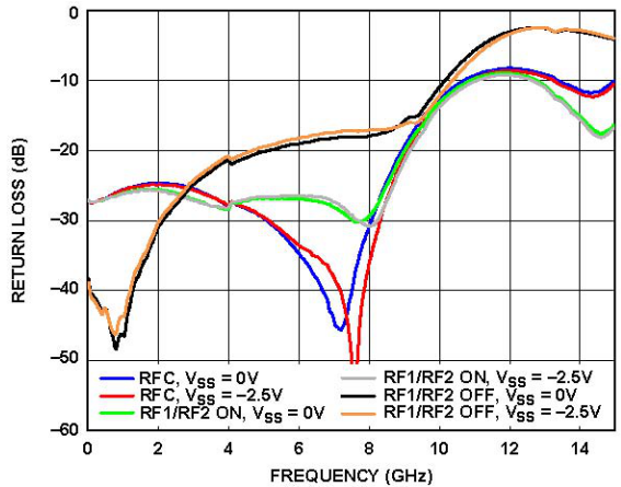
Figure 4. Return loss vs. frequency for different VSS values
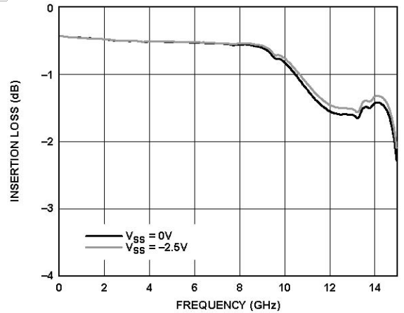
Figure 5. Insertion loss vs. frequency for different VSS values
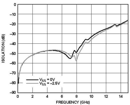
Figure 6. Isolation vs. frequency for different VSS
Large signal performance
The HMC1118 has several series FETs in both the series and shunt arms to withstand power levels above the breakdown voltage of a single FET. By evenly distributing the voltage across these FETs, the switch arm is optimized and achieves excellent linearity.
High RF power can modulate the gate voltage and drain-source channel resistance. This can cause intermodulation distortion and compression or clipping of the input signal. Biasing the FETs near the pinch-off level increases this effect.
Therefore, the power compression and linearity of the HMC1118 degrade when VSS changes from −2.5 V to 0 V, as shown in Figure 7 and Figure 8.
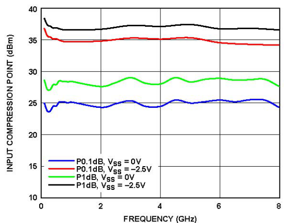
Figure 7. Input compression point vs. frequency for different VSS values
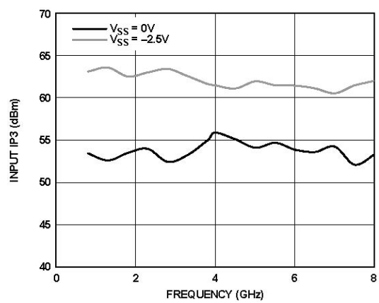
Figure 8. Input IP3 vs. frequency
switching time for different VSS
There is a trade-off between high power handling and fast switching times: larger gate resistors provide higher power handling capabilities at low frequencies, but switching times become slower. The HMC1118 optimizes the gate resistor value to provide high power handling capabilities at low frequencies while also having fast enough switching times.
The switching time performance of the HMC1118 degrades when VSS changes from −2.5 V to 0 V, as shown in Figure 9.
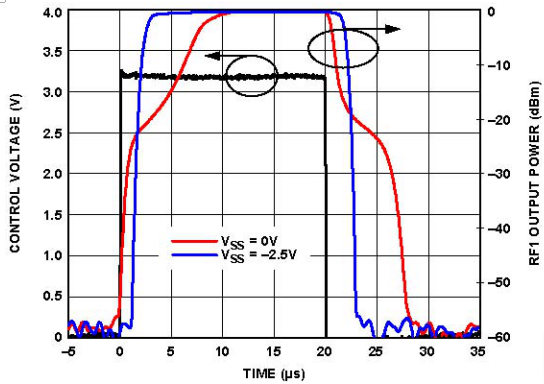
Figure 9. Switching time power handling at different VSS
As VSS changes from −2.5 V to 0 V, the HMC1118 maintains the same thermal characteristics but enters power compression at lower input power levels. The absolute and recommended maximum input power ratings for the HMC1118 RF port are derated due to the rapid increase in channel temperature.
Table 3. Maximum RF Input Power (PIN, MAX) Ratings1

VCTRL = 0 V or 3.3 V, TCASE = 85°C, f = 2 GHz.
Conclusion
When the HMC1118 is powered from a single positive supply of VDD = 3.3 V, power handling performance (PIN, MAX, P1dB, and IP3) is degraded, switching speed (turn-on and turn-off times and rise and fall times) is slower, but small signal characteristics (insertion loss, isolation, and return loss) are unchanged. If the reduced power handling and switching speed performance is acceptable for a particular application, the HMC1118 can be used with the VSS pin connected to ground.
Previous article:How to protect boost loads and their power supplies
Next article:Chemical battery charger supports maximum power point tracking for solar panels
Recommended ReadingLatest update time:2024-11-16 13:28


- MathWorks and NXP Collaborate to Launch Model-Based Design Toolbox for Battery Management Systems
- STMicroelectronics' advanced galvanically isolated gate driver STGAP3S provides flexible protection for IGBTs and SiC MOSFETs
- New diaphragm-free solid-state lithium battery technology is launched: the distance between the positive and negative electrodes is less than 0.000001 meters
- [“Source” Observe the Autumn Series] Application and testing of the next generation of semiconductor gallium oxide device photodetectors
- 采用自主设计封装,绝缘电阻显著提高!ROHM开发出更高电压xEV系统的SiC肖特基势垒二极管
- Will GaN replace SiC? PI's disruptive 1700V InnoMux2 is here to demonstrate
- From Isolation to the Third and a Half Generation: Understanding Naxinwei's Gate Driver IC in One Article
- The appeal of 48 V technology: importance, benefits and key factors in system-level applications
- Important breakthrough in recycling of used lithium-ion batteries
- Innolux's intelligent steer-by-wire solution makes cars smarter and safer
- 8051 MCU - Parity Check
- How to efficiently balance the sensitivity of tactile sensing interfaces
- What should I do if the servo motor shakes? What causes the servo motor to shake quickly?
- 【Brushless Motor】Analysis of three-phase BLDC motor and sharing of two popular development boards
- Midea Industrial Technology's subsidiaries Clou Electronics and Hekang New Energy jointly appeared at the Munich Battery Energy Storage Exhibition and Solar Energy Exhibition
- Guoxin Sichen | Application of ferroelectric memory PB85RS2MC in power battery management, with a capacity of 2M
- Analysis of common faults of frequency converter
- In a head-on competition with Qualcomm, what kind of cockpit products has Intel come up with?
- Dalian Rongke's all-vanadium liquid flow battery energy storage equipment industrialization project has entered the sprint stage before production
- Allegro MicroSystems Introduces Advanced Magnetic and Inductive Position Sensing Solutions at Electronica 2024
- Car key in the left hand, liveness detection radar in the right hand, UWB is imperative for cars!
- After a decade of rapid development, domestic CIS has entered the market
- Aegis Dagger Battery + Thor EM-i Super Hybrid, Geely New Energy has thrown out two "king bombs"
- A brief discussion on functional safety - fault, error, and failure
- In the smart car 2.0 cycle, these core industry chains are facing major opportunities!
- The United States and Japan are developing new batteries. CATL faces challenges? How should China's new energy battery industry respond?
- Murata launches high-precision 6-axis inertial sensor for automobiles
- Ford patents pre-charge alarm to help save costs and respond to emergencies
- New real-time microcontroller system from Texas Instruments enables smarter processing in automotive and industrial applications

 New concept analog circuit 1-5
 \"New Concept Analog Circuit\" - Transistor [Text Version] (Yang Jianguo)


 京公网安备 11010802033920号