The continuous innovation boom in the consumer electronics industry has led consumers to an unprecedented level of expectations for the speed of product technology improvement. Not only are products becoming more and more complex, but increasingly fierce competition has also greatly shortened the typical design cycle. Therefore, if a company can transform a product from a schematic to a product through an efficient design and testing process, it will have a competitive advantage in the industry.
While improving the development process often requires changes in the company, there are some practical tips that engineers can take to reduce time to market. This article not only explores how to achieve better manufacturing processes through simple design choices, but also discusses how to carefully select test software and hardware. The three most important best practices include:
• Design for manufacturability and debugging
• Write scalable and reusable test code
• Replicate the physical manufacturing environment at every stage of the development process
To understand the best practices from product design to product testing, we must consider that the purpose of production testing is often very different from that of design verification. Design verification testing is to verify that the product meets the specifications under various operating conditions. The purpose of production testing is to ensure that the product can be assembled correctly and the components are functioning properly. Despite the difference between these two purposes, engineers can apply verification test development to manufacturing through careful design. Note that although the best practices described here apply specifically to RF product development, the principles are applicable to any type of commercial product design.
Design for Manufacturability
In many companies, development teams often consider production testing only at the end of the design cycle. However, in order to use some of the results of the design phase in production, designers must anticipate possible problems with production testing from the early stages of the design. In many cases, if production testing is considered early in the design process, more appropriate decisions can be made on the layout and access of test signals/circuits, thereby reducing the overall cost of verification and production testing.
For example, it is often very difficult to add control circuits such as highly integrated ASICs to the initial design of a product. This requires expensive test equipment to simulate the operating environment of the device - resulting in longer test times and more expensive test costs. For example, the lack of non-signaling modes in mobile phone chips will greatly increase product verification time. If the initial design of the product does not include non-signaling modes, engineers will have to test the radio at a more expensive cost, and the simulation process of the base station will be greatly slowed down. Therefore, by adding key control circuits in the initial design of the product, engineers can shorten the time required for verification using lower-cost test equipment such as signal generators and signal analyzers.
One of the simplest ways to reduce potential production issues is to strictly adhere to design rules, such as component spacing, "keep-out areas," and correct pad shapes to prevent component "stand-ups." PCB manufacturers and chip manufacturers often provide design rule checking software to ensure that the product designed can actually be manufactured. It is very important to follow these design guidelines from the initial circuit layout. Although designers often tend to pay attention to design rules until late in the design, this delay often makes changes more difficult to achieve. On the other hand, engineers who pay attention to design rules from the initial design will design more reliable products and have an easier time transitioning from design to production.
Probing and debugging
A practical tip for identifying potential manufacturing issues in complex designs is to use the right debug and test interfaces. There are generally two main ways that engineers can improve their circuit testing, debugging, or troubleshooting capabilities. One approach is to add probe pads and various test interfaces to the product design. Another approach is to develop production-level test fixtures while working on the initial design to ensure more repeatable verification measurements.
During the development process, engineers often use manual probes to troubleshoot circuits. However, manual probes often introduce measurement errors and can cause engineers to make incorrect assumptions about circuit performance. Providing engineers with detailed information about product performance is critical during design and manufacturing. Therefore, designers must consider how to probe the performance of the system in a repeatable manner while minimizing the impact on the impedance of the circuit. Considering probing needs early in the design process can help ensure that the circuit layout and component placement facilitate engineers to properly probe performance.
Engineers are often reluctant to use board-to-board connectors due to cost. Probes can be a viable solution if engineers take attenuation into account and use the correct probe and pad pattern. For low-frequency (less than 100 MHz) applications, designers often use "spring" probes to measure signals on specific PCB traces. These probes, named for their spring mechanical action (similar to a pogo stick), work very well when used with the appropriate probe pads. However, for RF frequency applications, spring-type probes and pads are susceptible to a range of high-frequency-related parasitic behaviors that can affect electrical performance such as impedance matching and insertion loss.
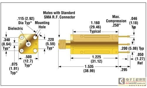
There are several probing solutions for RF and microwave frequencies, and one proven solution is to utilize a broadband coaxial probe. Coaxial probes, such as the Everett Charles K-50L shown here, have SMA connectors for easy connection to a spectrum analyzer or power meter. Although probes and probe pads can be used in many situations, RF engineers are often reluctant to use probe pads because they can create destructive capacitance that degrades circuit performance. A common solution is to design the probe pad based on the actual circuit board trace. For example, if the designer knows that an RF probe will be used later, the board geometry (such as trace width and ground plane spacing) can be designed for the probe without requiring a pad geometry of a specific shape. In some cases, surface mount component pads can be used as probe pads, allowing engineers to probe the circuit through a matching interface with the component removed.

Figure 1. Schematic diagram of the Everett Charles coaxial probe.
Another effective solution for validation and production testing is to use a coaxial connector with an integrated switch. In this approach, a single-pole double-throw switch is actuated by the mechanical action of the connection probe. Thus, the switch automatically wires to one terminal when the probe is not connected and to the other terminal when the probe is engaged. This integrated connector/switch probe was originally designed for the cell phone industry to disconnect the antenna to measure RF power through the connector. Today, RF engineers have a variety of high-performance devices to choose from at frequencies of 12 GHz and above.
Best Circuit Layout Practices
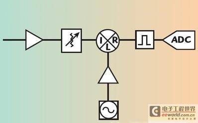
An important but often overlooked factor in design for manufacturability is the isolation of critical circuits, as shown in Figure 2, a block diagram of a typical receiver. To fully determine the performance of individual components, designers must be able to isolate the amplifier and mixer and the mixer from the local oscillator. If the synthesizer is not directly connected to the mixer through any interface to isolate the amplifier and mixer, it will make it more difficult to troubleshoot potential synthesizer failures. By separating these interfaces and testing each part independently, engineers can accurately troubleshoot with more complex components. There are several ways to separate the important interfaces. One method is to physically separate the layout of each subassembly and then connect them through coaxial connectors such as SMA. However, SMA connectors tend to increase the size and cost of the design. Integrated switch/connector assemblies, such as those described above, provide a good solution because they can well connect the amplifier, mixer and local oscillator with almost no insertion loss.
Figure 2. Typical transceiver architecture.
Correlate measurement data through reusable test code
Another problem that test engineers often face is correlating production data with measurements obtained during validation testing. Data correlation is difficult for several reasons, including the use of different test equipment, the effects of test fixtures, and changes in the physical environment. One of the easiest problems to solve is the error caused by the different measurement algorithms used for validation and engineering production testing.
Generally speaking, R&D teams usually need to have very high-performance equipment to ensure that the specification limits of the instrument do not affect the verification test results. The large number of instruments required for large-scale production operations usually requires the cost of production test equipment to be optimized. However, due to the different requirements of verification testing and production testing, companies often use completely different test equipment - resulting in problems such as measurement data cannot be correlated, and engineers need to spend extra effort to write test software.
Since differences between measurement algorithms can lead to differences in measurement results, one of the simplest steps to improve the correlation between verification and production testing is to ensure that all measurements are made using the same measurement algorithm. Engineers can ensure algorithm standardization through a number of methods, such as:
• Use software algorithms that run on the PC (or PXI system) rather than on the test instrument;
• Use similar test equipment (same vendor) for validation and production testing; • Use industry-defined measurements, such as those defined by IEEE standards.
The easiest way to ensure measurement algorithm standardization is to use instruments from the same vendor at all stages of product development. This approach also helps engineers more easily leverage test code used for validation testing during the production test phase.
Reuse verification test code for manufacturing testing
Although reusing validation test code in production may seem like an obvious best practice, it places special demands on software architecture. For example, a modular, layered software architecture is critical to leveraging code from design validation tests in production tests. When programming software for validation tests, engineers often ignore code architecture or long-term supportability in order to get the code out the door as quickly as possible. However, since many of the measurements required for validation tests are the same as for industrial tests, it is important to ensure that the validation test code is flexible.
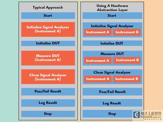
A simple best practice in writing test software code is to use a hardware abstraction layer. This approach encapsulates low-level driver calls for a specific device into higher-level functions. This approach makes it easier to modify the test code in the future to add additional devices without requiring a large-scale rewrite. As shown in Figure 3, using a hardware abstraction layer requires that the test code be architected so that the driver calls for a specific instrument are contained within the function call framework for that instrument product family. Although this requires more careful upfront design, using a hardware abstraction layer can increase the reuse of test code and ultimately reduce the time required to develop test software. Note that the hierarchy of the hardware abstraction layer is relatively straightforward compared to other programming languages that are inherently hierarchical, such as NI LabVIEW system design software or other similar languages.

Figure 3. Comparison of the traditional approach and the hardware abstraction layer approach. Note that an important aspect of the architecture shown in Figure 3 is the separation of the code that configures the device under test and the code that configures the instrument. Although the configuration of the device under test and the configuration of the instrument are often performed in parallel, it is better to separate these two tasks. In some cases, especially when test speed is the most important factor, the test executive software can automatically configure the two independent function calls to execute in parallel.
Verify and create consistency in the physical environment
The physical environment of an engineering lab is often very different from that of a manufacturing plant. Although it may seem counterintuitive, the environment in a manufacturing plant tends to vary far more than in a lab. Additionally, temperature variations, power quality issues, and even spurious responses from other equipment can affect test results. Therefore, a final best practice is to ensure that the physical environment during validation testing is exactly the same as that of the production plant.
While there are a variety of challenges in a production environment that can affect test results, temperature variation is probably the most significant. In a manufacturing plant, the high density of electronic equipment emits a large amount of constantly changing thermal radiation. In addition, other simple factors can also affect the local ambient temperature, such as the test equipment being located below the air conditioning outlet or near the door. Therefore, while an ideal manufacturing plant may have good control of the ambient temperature over a large area, it is still very difficult to control the local temperature of the device under test. These temperature changes will not only affect the accuracy of the equipment, but also greatly affect the performance of the device under test.
In my many years of manufacturing experience, I have personally observed factories that controlled the ambient temperature to within 1°C, but had local temperature fluctuations of up to 10°C at a particular test station. As an example of the impact of temperature on measurement quality, for a typical high-frequency amplifier, the power can change by 0.03 dB for every 1°C change in temperature. Instruments and complex equipment often use multiple amplifiers in a signal chain - so power errors caused by temperature changes will quickly accumulate. If the output power is to be adjusted to the smaller range required by the power amplifier, such as ±0.5 dB (or less), such large temperature changes will cause serious problems.
One of the best ways to reduce temperature changes caused by electromagnetic devices is to ensure good air circulation. In addition, it is very beneficial to measure temperature every time you make RF measurements (whether in the verification stage or the manufacturing stage). Especially in larger PCB designs, on-board temperature sensors are one of the effective ways to monitor temperature. By monitoring temperature, engineers can correlate each RF measurement with environmental conditions. Therefore, temperature data can often be used to explain the difference between verification and production test results.
Fixture
Another way to replicate the manufacturing environment during the validation phase is to use standardized fixtures. For many companies, fixtures are not considered until the production phase of the product development process. Although fixtures can have a positive or negative impact on measurement performance, it is very important to use fixtures that meet manufacturing requirements early in the development cycle. Fixture design and construction should be performed in parallel with early design or initial design.
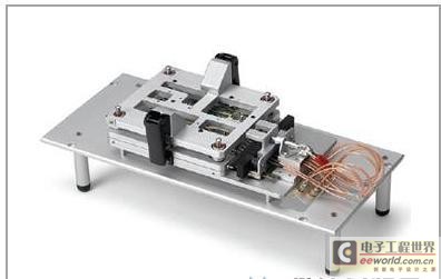
During the characterization phase, design test engineers often use poor wiring solutions, such as low-quality cables or connectors that are difficult to de-embed. Using high-quality fixtures for production testing at this stage has the following benefits. First, using fixtures during verification testing can improve measurement repeatability and stability, thereby improving measurement quality. Second, and more importantly, using better quality fixtures during verification often helps engineers better correlate verification test results with production test results. A board-level fixture is shown in Figure 4.

Figure 4. Board-level verification and manufacturing test fixture.
Fixtures that meet manufacturing requirements also allow engineers to test DUTs with minimal interaction with operators. Common manufacturing-grade fixtures provide repeatable interfaces for RF/analog measurements, control I/O, and DC power. In addition, fixtures can shield important environmental interference factors such as electromagnetic interference and have better heat dissipation. Fixtures can also minimize human hand contact – a factor that also affects the thermal characteristics of the product.
Electromagnetic Radiation
The final way to ensure consistency in the physical environment between validation and production is to measure and compensate (if necessary) the electrical environment. Generally speaking, there is less electrical interference in the validation lab. Since there are fewer products and electronic equipment to test in the lab than in the manufacturing plant, there are fewer interference factors. In some cases, if the validation lab uses a well-shielded enclosure, it can protect the DUT from external stray radiation.
When performing verification testing, an important best practice is to reproduce the manufacturing environment in the lab. For example, electromagnetic radiation interference can be measured using a spectrum analyzer, and then this interference can be reproduced using other DUTs in the verification lab. Other interference factors that need to be reproduced include power supply variations. When using manufacturing equipment in an environment where power supply stability is more important, it is particularly important to analyze the power supply. By simulating manufacturing tests during verification testing, engineers can predict the robustness of the test system and determine the impact on the test limits. This can prevent test problems that may occur in the early stages of manufacturing.
in conclusion
As the competition in the electronics industry becomes increasingly fierce, the ability to transition from product design to manufacturing test more quickly has become increasingly important to companies. As described in this article, engineers must improve their understanding of manufacturability design, test code development, and manufacturing environment conditions. Considering these factors in the early stages of design will help engineers significantly improve efficiency and quickly transition from product design to product manufacturing.
Bill Reid is the chief hardware architect at National Instruments and has 29 years of experience in the RF/microwave industry. He has extensive expertise in microwave product design, development and manufacturing test systems, customer consulting, and administrative management. He has been with NI for 12 years and has served as a business and technical manager. In addition to system and board-level design experience, Bill also has extensive metrology experience and is responsible for developing calibration processes and accuracy models for NI RF products. Prior to joining NI, Bill was employed by General Dynamics, EG&G, Texas Instruments, and Nokia Mobile Phones. Bill holds a bachelor's degree in electrical engineering from the University of Illinois at Chicago and a master's degree in electrical engineering from California State University, Fullerton.
Previous article:Design of 2GHz-4GHz comb-type ultra-wideband filter
Next article:Using twisted pair cables and low-pass filters to suppress RF and EMI
- Popular Resources
- Popular amplifiers
- MathWorks and NXP Collaborate to Launch Model-Based Design Toolbox for Battery Management Systems
- STMicroelectronics' advanced galvanically isolated gate driver STGAP3S provides flexible protection for IGBTs and SiC MOSFETs
- New diaphragm-free solid-state lithium battery technology is launched: the distance between the positive and negative electrodes is less than 0.000001 meters
- [“Source” Observe the Autumn Series] Application and testing of the next generation of semiconductor gallium oxide device photodetectors
- 采用自主设计封装,绝缘电阻显著提高!ROHM开发出更高电压xEV系统的SiC肖特基势垒二极管
- Will GaN replace SiC? PI's disruptive 1700V InnoMux2 is here to demonstrate
- From Isolation to the Third and a Half Generation: Understanding Naxinwei's Gate Driver IC in One Article
- The appeal of 48 V technology: importance, benefits and key factors in system-level applications
- Important breakthrough in recycling of used lithium-ion batteries
- LED chemical incompatibility test to see which chemicals LEDs can be used with
- Application of ARM9 hardware coprocessor on WinCE embedded motherboard
- What are the key points for selecting rotor flowmeter?
- LM317 high power charger circuit
- A brief analysis of Embest's application and development of embedded medical devices
- Single-phase RC protection circuit
- stm32 PVD programmable voltage monitor
- Introduction and measurement of edge trigger and level trigger of 51 single chip microcomputer
- Improved design of Linux system software shell protection technology
- What to do if the ABB robot protection device stops
- Huawei's Strategic Department Director Gai Gang: The cumulative installed base of open source Euler operating system exceeds 10 million sets
- Download from the Internet--ARM Getting Started Notes
- Learn ARM development(22)
- Learn ARM development(21)
- Learn ARM development(20)
- Learn ARM development(19)
- Learn ARM development(14)
- Learn ARM development(15)
- Analysis of the application of several common contact parts in high-voltage connectors of new energy vehicles
- Wiring harness durability test and contact voltage drop test method
- Two Application Examples of EPROM in Single Chip Microcomputer Development
- [Erha Image Recognition Artificial Intelligence Vision Sensor] Evaluation 1: Winner Chip Level Evaluation
- Circuit PCB Design
- What is Wi-Fi 6?
- 51 MCU software sharing, friends who want it can download it
- 【NUCLEO-L552ZE Review】+ Unboxing and lighting
- 【Download】STM32WB BLE application low power design
- MSP430F5529 Getting Started with Small Examples
- Qorvo's point-of-care diagnostic platform seems pretty good.
- Today's live broadcast: New requirements for connectors in 5G multi-scenario terminal applications and Molex's 5G connection solutions

 MAX9017AEKA


 京公网安备 11010802033920号