LED is a nonlinear device. A small change in forward voltage will cause a huge change in current. LED is a semiconductor diode. Its volt-ampere characteristic changes with temperature (-2mV/℃). If the temperature rises, the current of LED will increase under constant voltage drive. Long-term operation exceeding the rated current will greatly shorten the service life of LED. The main purpose of LED constant current is to ensure that its operating current remains unchanged when the input or output voltage changes. In order to ensure the advantages of LED products, for LED power supplies of different power ranges, it is necessary to select a suitable topology structure to make the LED driver power supply achieve high efficiency, high reliability, meet safety regulations, EMI- related standards and low cost requirements. For 15W-90W small and medium-power LED driver power supplies, a simple flyback topology is usually selected. According to the Class C standard of EN61000-3-2, all lighting products must meet its requirements, which has led to the rapid development of the single-stage PFC flyback architecture in the LED lighting market. Due to its high power conversion efficiency, low system cost and small size, it has been widely used in the field of LED lighting.
1 Working principle analysis and design
1.1TDA4863-2 chip introduction
TDA4863-2 is a power factor correction (PFC) controller launched by Infineon Semiconductor [1]. It works in quasi-resonant mode, the power factor can reach close to 1, the startup current is small, and the internal integrated totem pole can drive high-current MOSFET. TDA4863-2 is embedded with a current total harmonic distortion (THD) optimization circuit, which can effectively control the crossover distortion of the AC input current and the output ripple distortion of the error amplifier under full voltage input conditions, thereby improving the power factor and reducing the input current total harmonic distortion. This chip is mainly used in the pre-stage PFC correction circuit. In this article, it is applied to the single-stage PFC flyback architecture.
1.2 Design and principle analysis of single-stage flyback LED driver power supply based on TDA4863-2
The schematic diagram of the single-stage PFC flyback power supply of TDA4863-2 is shown in Figure 1. After passing through the EMI and rectifier units, the AC voltage flows into capacitor C1. The capacity of capacitor C1 can be a very small metallized film capacitor, so that the voltage across C1 has a 100Hz/120Hz waveform (depending on the input voltage frequency). The voltage can be approximately expressed as:

Where θ = ωt, VPK is the product of the input voltage and the square root of 2.
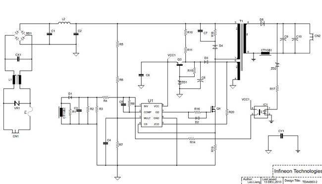
Figure 1: Critical mode single-stage PFC flyback circuit diagram
This voltage flows into the MULT pin of the IC after being divided by the resistors R5 and R6. The product of this voltage and the signal at the COMP pin is the output signal Vref of the internal multiplier. The output signal of the multiplier is also a full-wave rectified half-sine wave (error signal) after gain coefficient conversion, and is used as a reference for the input current.
When the switch is turned on, the inductor current IPKP in the primary winding NP rises linearly, and the CS pin detects the voltage of the resistor R19. When the voltage Vs across R19 rises to Vs=Vref, the voltage Vs across R19=IPKP*R19, and GD outputs a low-level signal to turn off the switch Q4.

In the waveform in Figure 2, Vref is the multiplier output signal, which is sent to the non-inverting input of the internal comparator, and the negative input is connected to the CS terminal. When GD outputs a high voltage, the MOSFET is turned on and the inductor current ramps up until the signal reaches the Vref level. At this point, the internal logic circuit changes state and makes GD output a low level, disconnecting the MOSFET, and the current ramps down until it drops to zero. The ZCD zero current detection circuit measures the voltage across the auxiliary winding (Nb). When its voltage drops to the ZCD threshold of 1.5V, at this moment, GD outputs a high level signal and the current ramps up again.
As can be seen from Figure 2, the primary inductor current changes in a triangular wave, the peak current envelope is a sine wave, and the current after the rectifier bridge is the average value of each triangular wave in the entire switching cycle, so its size is expressed as [2]:

Let K = Vpk/VR, D is the duty cycle, VR is the reflected voltage = turns ratio (N) * (Vout + VF)
From formula (3), we know that when K is 0, Iin(wt) is a sine wave, but as K increases, Iin(wt) deviates from the sine wave more seriously. Even in an ideal situation, the flyback topology cannot make the power factor 1. Since K is 0, the reflected voltage VR needs to be infinite. It can also be seen from formula (3) that if a higher power factor is to be obtained, a higher reflected voltage VR is required, that is, to increase the transformer turns ratio N=NP/NS, but due to the stress problem of MOSFET, the design of VR needs to be moderate, so that the rated voltage of MOSFET must be higher than the VDS voltage. In this design, the turns ratio n=3.8, the reflected voltage is about 190V, so an 800V MOSFET is selected.
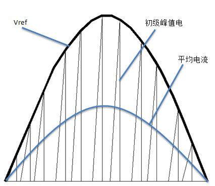
Figure 2: Primary current variation in a critical mode transformer
2. Constant current feedback analysis
The constant current feedback in this design is different from the common constant current feedback, as shown in Figure 4. This feedback design has the following advantages over the traditional constant current feedback circuit designed with CV/CC IC . First, it reduces the number of components and reduces the cost of BOM. Second, the feedback response time is fast and there is no overshoot. Third, this design has a short-circuit protection function. When the input is 300VAC, if the output is short-circuited, the measured input power is less than 1.8W, and the waveform is shown in Figure 3. When the secondary winding current increases and the current transformer detects that this current is higher than the preset value, the Vo terminal of CT1 outputs a high level to the INV pin of the IC, and the MOSFET is turned off (see Figure 3). Its working principle is to use a current transformer to detect the triangular wave current of the secondary winding, and send it to the INV pin of TDA4863-2 after rectification and filtering for precise current control.
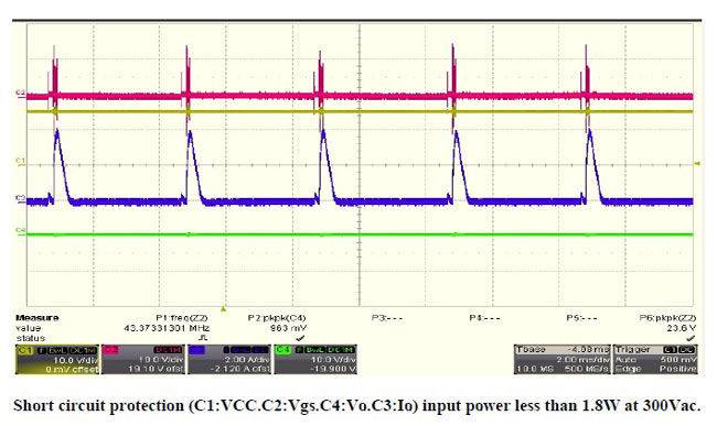
Figure 3: Output short-circuit protection waveform at 300Vac input

Figure 4: Output rectification filtering and constant current feedback circuit
3. Current transformer design
According to the characteristics of the current transformer, a core of high-? material is generally selected to make the excitation current as small as possible. The primary side usually selects 1 turn for easy operation. As Ns increases, the error of the current transformer decreases, and the loss of the sampling resistor also decreases. However, as Ns increases, the cost will also increase.
Known conditions: Vo=2.5V IP=1A
Assume: NP = 1TRo = 250 EUR
According to the formula NS=IP*NP/ISIs=Vo/Ro
Calculated: Ns = 100T
4. Experimental test and simulation data
The input in this design ranges from 85Vac to 300Vac, the output power is about 48W, the operating voltage is about 48V, and the output current is about 1A. Under standard load conditions, as shown in Figure 5, it can be seen that the two are very similar, and the input current waveform is basically a sine wave. From Figure 6, it can be seen that the power supply has a higher power factor, lower THD and high efficiency from 85V to 300V input, and the current accuracy error is less than +/-5%. The lower the input voltage, the higher the PF and the smaller the THD, which is consistent with the theoretical analysis of Formula 5. It can be seen that the lower the input voltage, the closer Iinθ is to the sine, the smaller the THD, and the higher the PF.
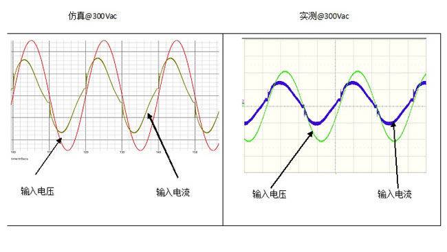
Figure 5: Power supply simulation and experimentally measured waveforms with 300Vac input
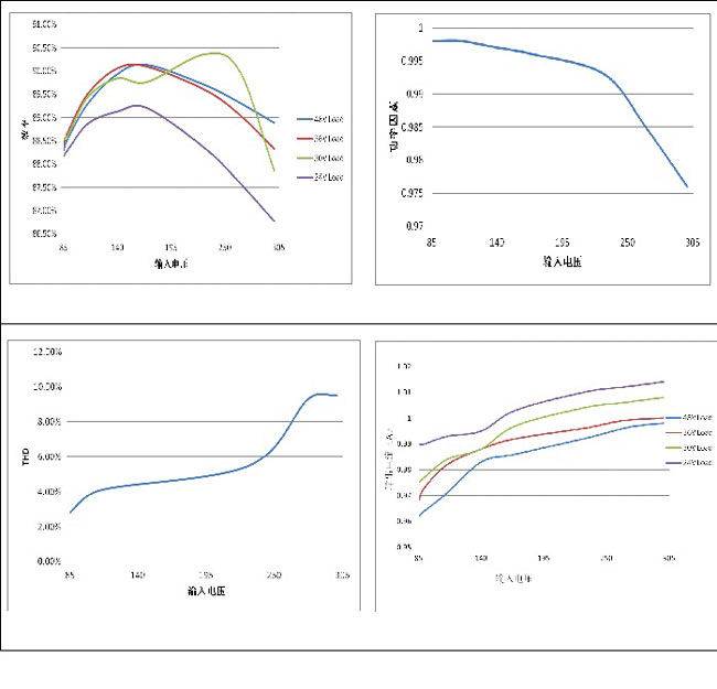
Figure 6: Power supply output characteristics for 85VAC-300VAC voltage input
5. Conclusion
This article introduces a single-stage PFC flyback LED driver based on TDA4863-2, and analyzes its working principle and how to achieve power factor theoretically. It also creates a model based on the SIMetrix/SIMPLIS simulation platform based on the schematic diagram in Figure 1 for system simulation. The power supply circuit has a simple structure. Through prototype experiments and simulation analysis, it is verified that the solution has high power factor, high efficiency, low THD, and good linear regulation and load regulation within the input voltage range of 85Vac-300Vac, and can well meet the technical requirements of EN61000-3-2 such as current harmonic components.
Previous article:High-power LED power supply solution based on LYTSwitch-4
Next article:Inventory: Comparison of several LED driving methods and selection of LED driving power supply
- Popular Resources
- Popular amplifiers
- MathWorks and NXP Collaborate to Launch Model-Based Design Toolbox for Battery Management Systems
- STMicroelectronics' advanced galvanically isolated gate driver STGAP3S provides flexible protection for IGBTs and SiC MOSFETs
- New diaphragm-free solid-state lithium battery technology is launched: the distance between the positive and negative electrodes is less than 0.000001 meters
- [“Source” Observe the Autumn Series] Application and testing of the next generation of semiconductor gallium oxide device photodetectors
- 采用自主设计封装,绝缘电阻显著提高!ROHM开发出更高电压xEV系统的SiC肖特基势垒二极管
- Will GaN replace SiC? PI's disruptive 1700V InnoMux2 is here to demonstrate
- From Isolation to the Third and a Half Generation: Understanding Naxinwei's Gate Driver IC in One Article
- The appeal of 48 V technology: importance, benefits and key factors in system-level applications
- Important breakthrough in recycling of used lithium-ion batteries
- LED chemical incompatibility test to see which chemicals LEDs can be used with
- Application of ARM9 hardware coprocessor on WinCE embedded motherboard
- What are the key points for selecting rotor flowmeter?
- LM317 high power charger circuit
- A brief analysis of Embest's application and development of embedded medical devices
- Single-phase RC protection circuit
- stm32 PVD programmable voltage monitor
- Introduction and measurement of edge trigger and level trigger of 51 single chip microcomputer
- Improved design of Linux system software shell protection technology
- What to do if the ABB robot protection device stops
- Keysight Technologies Helps Samsung Electronics Successfully Validate FiRa® 2.0 Safe Distance Measurement Test Case
- Innovation is not limited to Meizhi, Welling will appear at the 2024 China Home Appliance Technology Conference
- Innovation is not limited to Meizhi, Welling will appear at the 2024 China Home Appliance Technology Conference
- Huawei's Strategic Department Director Gai Gang: The cumulative installed base of open source Euler operating system exceeds 10 million sets
- Download from the Internet--ARM Getting Started Notes
- Learn ARM development(22)
- Learn ARM development(21)
- Learn ARM development(20)
- Learn ARM development(19)
- Learn ARM development(14)
- Overview of the process of drawing PCB with KiCad
- 08 IIC communication experience to obtain sensor data
- PADS9.5 Gerber screen printing changes to copper wire
- ADF4351 chip
- TMS320C6678 Development Routine User Manual Study Part 3
- QuartusII for Altera FPGA development example 1
- Basic knowledge of smart home technology
- A DIY DC to DC negative pressure module
- What is the purpose of the PG pin?
- DC-DC

 LM747CN


 京公网安备 11010802033920号