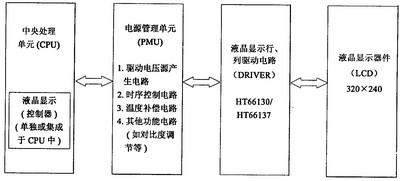
To realize the display of liquid crystal display, the following four units are required: controller, power management unit (PMU), driver circuit, liquid crystal display device (LCD). For liquid crystal display devices with smaller resolution, such as 128×64, 128×32 and other modules, there are chips that integrate controller, power management unit and driver. However, for high-resolution liquid crystal display (such as 320×240, 640×480), separate controller, power management unit and driver are required. This paper gives a design scheme of power management circuit for high-resolution liquid crystal display.
2 Circuit design scheme
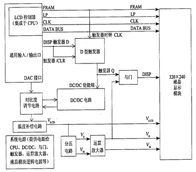
To realize liquid crystal display, four units are required, and its block diagram is shown in Figure 1. The power management circuit design scheme given in this paper has the functions of driving voltage generation, timing control, temperature compensation and contrast adjustment, and its block diagram is shown in Figure 2.
 |
|
Figure 1 Block diagram of the four units of the LCD system |
LCD display requires not only logic power supply but also driving power supply. The driving power supply varies with different driving chips. This article takes the HT66130/HT66137 of Hitachi, Japan as an example. This series of chips is a chip for driving high-resolution LCD displays, and the required driving voltages are VLCD, V0, and VM3. Since the duty cycle is 1/240 and the VLCD voltage is above 15V, we use the DC/DC device MAX1606 of Maxim to generate a 15.9V VLCD voltage, and obtain V0 and VM through resistor voltage division. V0 and VM are then provided to HT66130 and HT6613 through operational amplifiers, as shown in Figure 2.
 |
|
Figure 2 LCD power management block diagram |
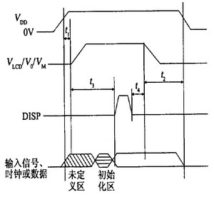
All LCDs have strict requirements for power-on and power-off timing. If the power-on and power-off timing do not meet the requirements, the display cannot be normal, and garbled characters, latching, residual display and other phenomena often occur. Taking the Japanese Hitachi driver chip HT66130/HT66137 driving a 320×240 LCD display as an example, the requirements for power-on and power-off timing are shown in Figure 3, and the requirements for general LCD driver chips are roughly the same.
Usually, the power management circuit of the LCD monitor relies on the CPU to use software to control the timing of the signal to ensure the power-on and power-off timing requirements of the LCD display device. This occupies more general input and output ports (GPIO), and the software has not yet run at the moment of power-on, and can only rely on the default state of the CPU's GPIO to control. At present, dual-CPU systems such as smart phones are more difficult to control by software. The circuit designed in this article only needs one GPIO (i.e., the display enable signal DISP) to control the power-on and power-off timing and the switch of the driving power supply, and there is no timing requirement for DISP.
 |
|
Figure 3 Hitachi HT66130/HT66137 timing diagram |
For the power-on timing, generally, there must be a frame frequency initialization time before the display enable signal can be set to a high level. The traditional approach is to rely on the CPU's GPIO port delay to control. The circuit designed in this article uses a D-type flip-flop, and uses the frame frequency signal (FRAME) as the clock input, the display enable signal (DISP) as the D input and controls the CLEAR end, and the Q end output controls the switch of the entire drive circuit. In this way, the timing control of the DISP input can be realized, and the DISP can be used to control the switch of the entire drive power circuit. Since the DISP can turn off the drive circuit, the standby state can be realized. The power consumption of the drive circuit is very small, and there is only the static current of the trigger and gate circuit. In order to meet the DISP signal input after the drive voltage is stable, we use the AND gate to control the DISP and the drive voltage input to realize the DISP output.
When powering off, the timing of the display enable signal, drive power, display clock/data signal, and logic power must be strictly followed. In order to meet the power-off timing requirements, the CPU's GPIO is generally used for control. This design uses a D flip-flop and an AND gate to realize that the DISP is set low in advance of the drive voltage. The DISP signal is used to control the power supply circuit. When DISP is set low, the driving power supply of the HT66130/HT66137 driver chip is completely turned off, and no additional GPIO port is required for control. The test shows that the circuit operates normally and can effectively control the timing of power on and off, without garbled code, latching, residual display and other phenomena. Moreover, the power consumption of the driving circuit in the standby state is very small, only 0.2 mW (including circuit and LCD display device).
2. 3 Temperature compensation circuit
In order to ensure that the LCD display can work normally in a wide temperature range, the temperature compensation circuit is very necessary. The driving voltage and temperature characteristics of the LCD screen used are shown in the solid line of Figure 4. Therefore, the circuit design is optimized by using the temperature characteristics of thermistors and the series-parallel relationship of resistors. The specific circuit is shown in Figure 5. R1=638 kΩ, R2=110 kΩ, R3=62 kΩ, and the characteristics of RTH are shown in Table 1. The calculation formula of R1, R2, R3, RTH and DC/DC (MAX1606) output voltage is:
|
Figure 4 LCD screen temperature compensation curve |
The contrast adjustment of the LCD can be divided into hardware adjustment and software adjustment. The circuit in Figure 5 has both software and hardware adjustment functions. R1 is an adjustable resistor that can adjust the voltage of VLCD, so that the contrast of the LCD can be adjusted; the circuit can also use the CPU combined with the digital-to-analog converter (DAC) to control the voltage at the feedback end of the DC/DC, so as to achieve software adjustment of the contrast of the LCD.
|
Figure 5 Temperature compensation/contrast adjustment circuit |
The test flow chart of LCD startup and shutdown is shown in Figure 6. The initialization of the LCD controller is the most important, and the CPU registers and delay time must be configured according to the requirements of the LCD display module.
|
Figure 6 LCD display software flow chart |
4 Conclusion
The actual test shows that the circuit operates normally and can effectively control the timing of power on and off. The power consumption of the drive circuit in the standby state is only 0.2mW. The temperature compensation characteristics are good. Both software and hardware can adjust the contrast of the LCD display.
Previous article:Reducing Power Supply Noise in High-Speed DSP System Design
Next article:Circuit Design of LCD Power Management
Recommended ReadingLatest update time:2024-11-16 16:54

- MathWorks and NXP Collaborate to Launch Model-Based Design Toolbox for Battery Management Systems
- STMicroelectronics' advanced galvanically isolated gate driver STGAP3S provides flexible protection for IGBTs and SiC MOSFETs
- New diaphragm-free solid-state lithium battery technology is launched: the distance between the positive and negative electrodes is less than 0.000001 meters
- [“Source” Observe the Autumn Series] Application and testing of the next generation of semiconductor gallium oxide device photodetectors
- 采用自主设计封装,绝缘电阻显著提高!ROHM开发出更高电压xEV系统的SiC肖特基势垒二极管
- Will GaN replace SiC? PI's disruptive 1700V InnoMux2 is here to demonstrate
- From Isolation to the Third and a Half Generation: Understanding Naxinwei's Gate Driver IC in One Article
- The appeal of 48 V technology: importance, benefits and key factors in system-level applications
- Important breakthrough in recycling of used lithium-ion batteries
- Innolux's intelligent steer-by-wire solution makes cars smarter and safer
- 8051 MCU - Parity Check
- How to efficiently balance the sensitivity of tactile sensing interfaces
- What should I do if the servo motor shakes? What causes the servo motor to shake quickly?
- 【Brushless Motor】Analysis of three-phase BLDC motor and sharing of two popular development boards
- Midea Industrial Technology's subsidiaries Clou Electronics and Hekang New Energy jointly appeared at the Munich Battery Energy Storage Exhibition and Solar Energy Exhibition
- Guoxin Sichen | Application of ferroelectric memory PB85RS2MC in power battery management, with a capacity of 2M
- Analysis of common faults of frequency converter
- In a head-on competition with Qualcomm, what kind of cockpit products has Intel come up with?
- Dalian Rongke's all-vanadium liquid flow battery energy storage equipment industrialization project has entered the sprint stage before production
- Allegro MicroSystems Introduces Advanced Magnetic and Inductive Position Sensing Solutions at Electronica 2024
- Car key in the left hand, liveness detection radar in the right hand, UWB is imperative for cars!
- After a decade of rapid development, domestic CIS has entered the market
- Aegis Dagger Battery + Thor EM-i Super Hybrid, Geely New Energy has thrown out two "king bombs"
- A brief discussion on functional safety - fault, error, and failure
- In the smart car 2.0 cycle, these core industry chains are facing major opportunities!
- The United States and Japan are developing new batteries. CATL faces challenges? How should China's new energy battery industry respond?
- Murata launches high-precision 6-axis inertial sensor for automobiles
- Ford patents pre-charge alarm to help save costs and respond to emergencies
- New real-time microcontroller system from Texas Instruments enables smarter processing in automotive and industrial applications
- KiCad Production File Generator
- [AT-START-F403A Evaluation] 3. QR code routine verification under Keil environment
- TI Cup 2019 National Undergraduate Electronic Design Competition Retest Notice (Retest List Has Been Announced):
- TMS320F280049C Study Notes 15 DAC
- What if the uploaded image is not used? See here
- [Xingkong Board Python Programming Learning Main Control Board] Flip Tomato Clock
- How to send more than 20 bytes of data at a time with blue_nrg
- I stayed up late to sort it out. Here is the servo information on the national competition list.
- How to make an overvoltage protection circuit?
- Detailed explanation of starting surge current

 Circuit Intuition
 Signal Integrity and Power Integrity Analysis (Eric Bogatin)
 Arduino DUE drives Adafruit Sharp Memory Display Breakout screen
 【Digi-Key Electronics Follow me 4th Mission Result Code


 京公网安备 11010802033920号