Digital potentiometers (digiPOTs) are often used to easily adjust the AC or DC voltage or current output of sensors, power supplies, or other devices that require some type of calibration, such as timing, frequency, contrast, brightness, gain, and offset adjustment. Digital settings can avoid almost all the problems associated with mechanical potentiometers, such as physical size, mechanical wear, wiper setting, resistance drift, and sensitivity to vibration, temperature, and humidity. It can also eliminate the inflexible layout caused by the use of a screwdriver.
The digiPOT can be used in two modes, potentiometer mode or variable resistor mode. Figure 1 shows the potentiometer mode, where there are three terminals, the signal is connected through terminals A and B, and terminal W ( similar to a wiper ) provides an attenuated output voltage. When the digital ratio control input is all zero, the wiper is usually connected to terminal B.

Figure 1. Potentiometer mode
When the wiper is hardwired to either end, the potentiometer becomes a simple variable resistor , as shown in Figure 2. The variable resistor mode requires fewer external pins and is therefore smaller. Some digiPOTs are available in variable resistor mode only.

Figure 2. Variable resistor mode
There is no restriction on the polarity of the current or voltage at the resistor terminals of a digiPOT, but the amplitude of the AC signal cannot exceed the power supply rails (VDD and VSS ) . When the device is operating in variable resistor mode, especially at low resistance settings, the maximum current or current density should be limited.
Typical Applications
Signal attenuation is an inherent characteristic of the potentiometer mode because the device is essentially a voltage divider. The output signal is defined as:
V
OUT
= V
IN
× (
R
DAC
/R
POT
), where
R
POT
is the nominal end-to-end resistance of the digiPOT and
R
DAC
is the digitally selected resistance between the W terminal and the input signal reference pin, which is usually the B terminal, as shown in Figure 3.

Figure 3. Signal attenuator
Signal amplification requires an active device, usually an inverting or non-inverting amplifier. With the appropriate gain formula, either potentiometer mode or variable resistor mode can be used
Figure 4 shows a non-inverting amplifier, where the digiPOT acts as a potentiometer and the gain can be adjusted by feedback. Since part of the output is fed back, R AW / ( R WB + R AW ), should be equal to the input, and the ideal gain is:

Figure 4. Noninverting amplifier in potentiometer mode.
The gain of this circuit is inversely proportional to R AW , and rises rapidly as R AW approaches zero, exhibiting a hyperbolic transfer function characteristic. To limit the maximum gain, a resistor can be inserted in series with R AW (which is in the denominator of the gain formula).
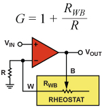
If a linear gain relationship is desired, the variable resistor mode can be used with fixed external resistors, as shown in Figure 5, and the gain is now defined as:

Figure 5. Noninverting amplifier in rheostat mode.
For best performance, connect the low capacitance terminal (W pin in newer devices) to the op amp input.
Advantages of digiPOTs for signal amplification
The circuits shown in Figures 4 and 5 have high input impedance and low output impedance and can operate with unipolar and bipolar signals. The digiPOT can be used for vernier operation, providing higher resolution over a smaller range with fixed external resistors, and can be used in op amp circuits with or without signal inversion. In addition, the digiPOT has a low temperature coefficient, typically 5 ppm/°C in potentiometer mode and 35 ppm/°C in variable resistor mode.
Limitations of digiPOTs for signal amplification
When processing AC signals, the performance of a digiPOT is limited by bandwidth and distortion. Bandwidth is the maximum frequency that can pass through the digiPOT with less than 3 dB attenuation due to parasitic components.
Total harmonic distortion
(THD), defined here as the ratio of the rms sum of the last four harmonics to the output fundamental, is a measure of the attenuation of the signal as it passes through the device. These specifications involve performance limitations that are determined by the internal digiPOT architecture. Through analysis, we can better understand these specifications overall and reduce their negative impact.
The internal architecture has evolved from the traditional series resistor array (shown in Figure 6a) to a segmented architecture (shown in Figure 6b). The main improvement is the reduction in the number of internal switches required. In the first case, a serial topology is used with N = 2 switches where n is the number of bits of resolution. For n = 10, 1024 switches are required .

Figure 6. a) Traditional architecture, b) Segmented architecture
The proprietary (patented) segmented architecture uses cascade connections to minimize the total number of switches. The example in Figure 6b shows a two-segment architecture consisting of two types of blocks, the MSB on the left and the LSB on the right.
The left upper and lower blocks are a string of switches for coarse bit adjustment (MSB segment). The right block is a string of switches for fine bit adjustment (LSB segment). The MSB switches roughly adjust the ratio close to R A /R B. The total resistance of the LSB string is equal to the single resistive element in the MSB string, and the LSB switches can finely adjust the ratio at any point on the main switch string. The A and B MSB switches are complementary codes.
The number of switches for the segmented architecture is:
N = 2 m + 1 + 2 n – m ,
Where n is the total number of bits and m is the number of bits of resolution for the MSB word. For example, if n = 10 and m = 5, 96 switches are required.
The segmented solution requires fewer switches than traditional switch strings:
The difference in the number of switches between the two = 2n – (2m + 1 + 2n – m )
In this example, the savings are
1024 – 96 = 928!
Both architectures must select switches with different resistance values to account for the AC error sources in analog switches. These CMOS (complementary metal oxide semiconductor) switches are constructed from parallel P-channel and N-channel MOSFETs. This basic bidirectional switch maintains a fairly constant resistance ( R ON ) for signals up to the full supply rails.
Bandwidth
Figure 7 shows the parasitic components that affect the AC performance of a CMOS switch.

Figure 7. CMOS switching mode.
C DS = drain-source capacitance; C D = drain-gate + drain-bulk capacitance; CS = source-gate + source-bulk capacitance.
The transfer relationship is defined as follows, which contains the following assumptions:
- Source impedance is 0 Ω
- No external load influence
- No impact from CDS
- R LSB << R MSB

in:
R DAC is the setting resistor
R POT is the end-to-end resistance
C DLSB is the total drain-gate + drain-bulk capacitance of the LSB segment
C SLSB is the total source-gate + source-bulk capacitance of the LSB segment
C DMSB is the drain-gate + drain-bulk capacitance of the MSB switch
C SMSB is the source-gate + source-bulk capacitance of the MSB switch
moff is the number of open switches in the MSB path of the signal
m on is the number of switches turned on in the MSB path of the signal
The transfer formula is affected by various factors and is somewhat related to the code, so we use the following additional assumptions to simplify the formula
C DMSB + C SMSB = C DSMSB
C DLSB + C SLSB >> C DSMSB
( C DLSB + C SLSB ) = C W (See data sheet for details)
The CDS has no effect on the transfer equation, but since its frequency of occurrence is usually higher than the poles, the multi- RC low-pass filter is the dominant response. The ideal approximation is simplified to:
Bandwidth ( BW ) is defined as:
Where C L is the load capacitance.
see catalog ). Figure 8 shows the effect of low-pass filtering, which is code dependent and varies for different nominal resistance and load capacitance values.

Figure 8. Maximum bandwidth vs. load capacitance for various resistor values
The parasitic trace capacitance of the PC board should also be considered, otherwise the maximum bandwidth will be lower than expected. The trace capacitance can be simply calculated using the following formula:
in
ε R is the dielectric constant of the plate
A is the routing area (cm 2 )
d is the interlayer distance (cm)
For example, assuming that the FR4 board has two signal layers and a power/ground layer, ε R = 4, trace length = 3 cm, width = 1.2 mm, and layer spacing = 0.3 mm; the total trace capacitance is approximately 4 pF.
Distortion
THD is used to quantify the nonlinearity of the device as an attenuator. This nonlinearity is caused by the internal switches and their voltage-dependent on-resistance
R
ON
. Figure 9 shows an amplified example of amplitude distortion.

Figure 9. Distortion
Compared to a single internal passive resistor, the R ON of the switch is small and its variation over the signal range is even smaller. Figure 10 shows a typical on-resistance characteristic.

Figure 10. CMOS resistor
The resistance curve depends on the supply voltage rail, with the internal switch's R ON variation being minimal at maximum supply voltage . As the supply voltage decreases, R ON variation and nonlinearity increase. Figure 11 compares the R ON of a low-voltage digiPOT at two supply levels.

Figure 11. Switch resistance change vs. supply voltage
HD depends on various factors and is therefore difficult to quantify, but assuming a 10% change in R ON , the following formula can be used for an approximate calculation:
Generally speaking, the larger the nominal digiPOT resistance ( R POT ), the larger the denominator and the smaller the THD.
As R
POT
increases
, both distortion and bandwidth decrease, so improving one metric necessarily sacrifices the other. Therefore, circuit designers must make the appropriate trade-off between the two. This also relates to the design level of the device, because IC designers must balance the various parameters in the design formula:
in
C OX is the oxide capacitor
μ is the migration constant of electrons (NMOS) or holes (PMOS)
W is the width
L is the length
Biasing
From a practical point of view, we must make the most of each characteristic. When the digiPOT attenuates an AC signal through capacitive coupling, distortion is minimized if the signal is biased to the midpoint of the power supply. This means that the switch operates in the most linear part of the resistance characteristic.
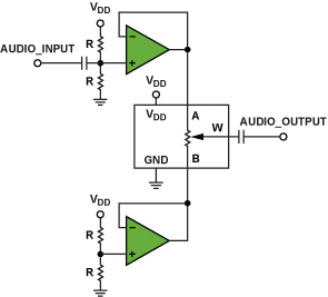
One method is to use dual supplies and simply ground the potentiometer to the common mode of the power supplies to produce positive and negative swings in the signal. If single supply operation is required, or some digiPOTs do not support dual supplies, another method can be used, which is to add an offset voltage of V DD /2 to the AC signal. This offset voltage must be added to both resistor terminals, as shown in Figure 12.

Figure 12. Single-supply AC signal conditioning
If a signal amplifier is required, a dual-supply inverting amplifier is preferred over a non-inverting amplifier (as shown in Figure 13) for two reasons:
- THD performance is better because the virtual ground at the inverting pin centers the switch resistance in the middle of the voltage range.
- Because the inverting pin is located at the virtual ground, the wiper capacitor C DLSB is almost eliminated , resulting in a smaller bandwidth increase (circuit stability must be noted).

Figure 13. Adjustable amplification using an inverting digiPOT amplifier
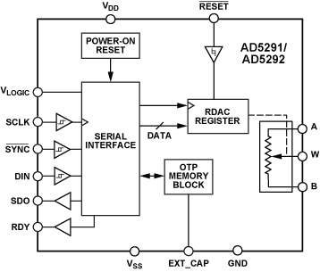
The AD5291 / AD5292 digital potentiometers, shown in Figure 14, feature 256/1024-position resolution. End-to-end resistance is available in 20 kΩ, 50 kΩ, and 100 kΩ with better than 1% error and a temperature coefficient of 35 ppm/°C in variable resistor mode and 5 ppm/°C (ratio) in voltage divider mode. These devices perform the same electronic adjustment function as mechanical potentiometers, but are smaller and more reliable. Their wiper position is adjustable via an SPI-compatible interface. An unlimited number of adjustments can be made before the wiper position is fixed by blowing the fuse (a process similar to applying epoxy to a mechanical trimmer). The “epoxy removal” process can be repeated up to 20 times. The AD5291/AD5292 operates from a single 9 V to 33 V supply or dual ±9 V to ±16.5 V supplies and consumes 8 μW. Available in 14-Lead TSSOP Package and Operates from –40°C to +105°C ( Back to Content )

Figure 14. AD5291/AD5292 functional block diagram
| About the Author | |

|
Miguel Usach Merino
[
miguel.usach@analog.com
] received his degree in electronic engineering from the University of Valencia. He joined Analog Devices in 2008 as an applications engineer in the Precision DAC Group in Limerick, Ireland.
|
Previous article:Topology and application trends of ultra-low dropout linear regulators
Next article:Multifunctional inverter and rectifier circuit in power electronics technology
- Popular Resources
- Popular amplifiers
-
 Mission-oriented wireless communications for cooperative sensing in intelligent unmanned systems
 -
 CVPR 2023 Paper Summary: Embodied Vision: Active Agents, Simulation
 -
 ICCV2023 Paper Summary: Fairness, Privacy, Ethics, Social-good, Transparency, Accountability in Vision
 -
 Introduction to Artificial Intelligence and Robotics (Murphy)
- MathWorks and NXP Collaborate to Launch Model-Based Design Toolbox for Battery Management Systems
- STMicroelectronics' advanced galvanically isolated gate driver STGAP3S provides flexible protection for IGBTs and SiC MOSFETs
- New diaphragm-free solid-state lithium battery technology is launched: the distance between the positive and negative electrodes is less than 0.000001 meters
- [“Source” Observe the Autumn Series] Application and testing of the next generation of semiconductor gallium oxide device photodetectors
- 采用自主设计封装,绝缘电阻显著提高!ROHM开发出更高电压xEV系统的SiC肖特基势垒二极管
- Will GaN replace SiC? PI's disruptive 1700V InnoMux2 is here to demonstrate
- From Isolation to the Third and a Half Generation: Understanding Naxinwei's Gate Driver IC in One Article
- The appeal of 48 V technology: importance, benefits and key factors in system-level applications
- Important breakthrough in recycling of used lithium-ion batteries
- Innolux's intelligent steer-by-wire solution makes cars smarter and safer
- 8051 MCU - Parity Check
- How to efficiently balance the sensitivity of tactile sensing interfaces
- What should I do if the servo motor shakes? What causes the servo motor to shake quickly?
- 【Brushless Motor】Analysis of three-phase BLDC motor and sharing of two popular development boards
- Midea Industrial Technology's subsidiaries Clou Electronics and Hekang New Energy jointly appeared at the Munich Battery Energy Storage Exhibition and Solar Energy Exhibition
- Guoxin Sichen | Application of ferroelectric memory PB85RS2MC in power battery management, with a capacity of 2M
- Analysis of common faults of frequency converter
- In a head-on competition with Qualcomm, what kind of cockpit products has Intel come up with?
- Dalian Rongke's all-vanadium liquid flow battery energy storage equipment industrialization project has entered the sprint stage before production
- Allegro MicroSystems Introduces Advanced Magnetic and Inductive Position Sensing Solutions at Electronica 2024
- Car key in the left hand, liveness detection radar in the right hand, UWB is imperative for cars!
- After a decade of rapid development, domestic CIS has entered the market
- Aegis Dagger Battery + Thor EM-i Super Hybrid, Geely New Energy has thrown out two "king bombs"
- A brief discussion on functional safety - fault, error, and failure
- In the smart car 2.0 cycle, these core industry chains are facing major opportunities!
- The United States and Japan are developing new batteries. CATL faces challenges? How should China's new energy battery industry respond?
- Murata launches high-precision 6-axis inertial sensor for automobiles
- Ford patents pre-charge alarm to help save costs and respond to emergencies
- New real-time microcontroller system from Texas Instruments enables smarter processing in automotive and industrial applications
- ARM's strategic layout in the field of Internet of Things
- BearPi-HM Nano Development Board Review 1 Getting Started with Program Development
- I have some doubts about SensorTile.box
- A novice needs help. When drawing PCB manual wiring in AD13.4, why can't I see the trace of the wiring before the wiring is completed?
- What are the important techniques for PCB wiring?
- Naming of Cadence Allegro 17.2 built-in pads
- A precision rectification experiment
- Video: Talking about TI CC2650
- How stable is RT-Thread?
- How to improve the hardware and software architecture of embedded minimum systems?


 Mission-oriented wireless communications for cooperative sensing in intelligent unmanned systems
 CVPR 2023 Paper Summary: Embodied Vision: Active Agents, Simulation


 京公网安备 11010802033920号